This thread has been locked.

If you have a related question, please click the "Ask a related question" button in the top right corner. The newly created question will be automatically linked to this question.

DP83869HM: Schematic Review -DP83869PHY_FO interface section

Part Number: DP83869HM

Hi Sir,

I have attached the schematic design  DP83869PHY chip and AFBR-5803 interface section with the following configuration also.

Please find the below PHY configuration details and confirm the configuration is correct or not

  1.  Device PWR supply is 2 supply configuration but considered 1.8V section is  "No-load" in the design.
    Please confirm the 1.8VDC bus is required for the 100FX fiber interface. The used supply voltage in the design is 3.3VDC, 2.5VDC & 1.1VDC.
  2. Whether  AC coupling capacitor is required for FX OUTPUT signal to Fiber transceiver module. Please check the 0.1uF added on the AFBR-5803 is OK or not. 
  3. PIN 24, JTAG_TDI pin configured as "Signal detect " of SC-FO transceiver. Provide pull-up to the  LED1(pin-46 of IC) to configure the pin to "SD". Also please check the resistor value used for pull-up the  4.7K pin is OK or not.
  4.  LED0 used for FO auto-negotiation. Please check the configuration also.
  5. Please confirm the RGMII to 100FX mode section resistor configuration. Also, crosscheck the resistor values are OK or Not.
  6. Please confirm the PHY address configuration of  "1010" is using resistor strap and resistor values are ok. 
  7. Please confirm the unused JTAG pins need to pull-up or Pull Down
  8. How to set the LED one for FO to connection detect and the other for FO Activity module. It is set through software or the PIN strap method. Please confirm.
  9. How to disable the CLKOUT.

Please find the attached schematic.DP83869PHY_100FX SC_FO.pdfDP83869PHY_100FX SC_FO.pdf

  • Hello,

    I am in the process of reviewing the schematic and will look at the configuration details you have listed. I will get back to you at the latest by end of day Wednesday with comments I have on the schematic.

    Regards,

    Adrian Kam

  • Hello,

    Below are my comments on your schematic:

    1. 1.8VDC is not required for 100FX fiber interface. If you are using a two supply configuration, then what you have in the schematic should be fine. You can use either two supply or three supply configuration for RGMII to 100FX mode.
    2. The 0.1uF AC coupling capacitors are OK.
    3. The configuration is fine, but the strap resistor should be 2.49K.
    4. Since your current configuration is set to RGMII to 100FX mode, there is no auto-negotiation configuration, so it does not do anything. If you were to switch to RGMII to 1000X mode, then the auto-negotiation strap configuration is correct, but the strap resistor should be 2.49K. Refer to section 9.5.1.4 and 9.5.1.5 of the datasheet for details.
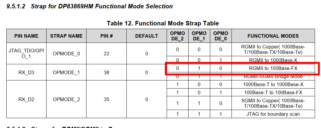
    5. Mode selection strap configuration is correct, but the strap resistor should be 2.49K.
    6. PHY address configuration is good, and the resistor values are good.
    7. The unused JTAG pins can be left unconnected.
    8. LED function can be set in register 0x18. Also, refer to figure 31 of section 9.5.2 of the datasheet on how to connect the LEDs with strap resistors.
    9. CLKOUT can be disabled by setting bit[6] = 1 of register 0x170.

    Other comments outside of your list:

    1. Chassis GND should be connected to GND with a 4.7nF capacitor, along with a 1M resistor in parallel with the capacitor.
    2. MDIO and Reset pin should be pulled up to VDDIO using a 2.2K resistor.
    3. Instead of 10uF decoupling capacitor, we recommend 1uF as mentioned in the datasheet.
    4. Except for the PHY address straps, the resistor value of straps should be 2.49K. See section 9.5.1 of the datasheet for more details.

    Regards,

    Adrian Kam

  • Dear Mr.Adrian Khan,

    In my application the boot strap resistors are 2.7k instead of 2.49K. But I am able to read the strap registers correctly.

    But I am not able to get the link. DO you think that the 2.49K resistor might be a problem.

    Regards

    Hemanth R

  • Hi Hemanth,

    If you are reading the strap registers correctly, then 2.7k should be fine. What is important is that the target voltage is within spec as shown in the datasheet.

    As for your link problem, we would be happy to help you with it if you can start another thread. That way, this thread does not become cluttered.

    Regards,

    Adrian Kam

  • Hi Adrian Kam,

    Please check my comments  SCHEMATIC1 _ 03 PHY_100FX SC_FO (1).pdf

    1. We planed to use two PWR supply mode. I have to keep 1.8V components are "No load" in the design 
    2. OK, Fiber is connected in SGMII/Fiber data line.
    3. OK, the Strap resistor value changed to 2.49K( Pin #46- LED1 ).
    4. I have connected Pin# 47to GND in the schematic through 2.49K resistor. But in the datasheet 9.5.1.5 section mentioned only PIN#46 for SD control for 100Fx.
      So please confirm whether autonegotionation is required in 100FX mode. If yes please share the required configuration.
    5. Mode selection strap changed to 2.49K.
    6. OK,PHY address configuration.
    7. OK, i have kept the JTAG pins to left open.
    8. Also please confirm the following differential signal kept open or pulled down to GND.Pin # 1,2,4,5,7,8,10 & 11.
    9. OK, i have planned to use LED0 and LED1 for Link and TX/RX activity of FO. please confirm how to set the LEDs inactive low using the Register setting. We have already connected strap resistors in the same LED pins.
    10. OK, I will set the in CLKOUT register to disabled 
    11. OK, I have connected 4.7nF and 1M to Chassis GND.
    12. OK, added 2.2K MDIO and Reset pins. The added resistor in Connector schematic sheet in design.
    13. OK, Changed 10uF to 1uF cap in the PWR line.

    For more details, i have attached the updated Schematic.

  • Hello,

    The schematic you attached seems to be the same one as before. Here are my comments.

    1. Yes, 1.8V components should be "no load" or "no connect" in the design.
    2. Auto-negotiation is not required for 100FX mode. Configuring the strap on pin 47 will do nothing.
    3. The differential signals can be kept open.
    4. You cannot set LED functions using straps; it has to done using register writes. If you look at register 0x18, it provides details on what bits to set to achieve your desired functions. Setting bits[3:0] = 0x0 configures LED0 for Link, and setting bits[7:4] = 0x1 configures LED1 for TX/RX Activity.

    It seems you have made all the changes I suggested in the previous reply based on your list. In that case, your schematic should be good. I can still take one final look if you attach the updated schematic.

    Regards,

    Adrian Kam

  • Hi Adrian Kam,

    Please replay the below comments also. 

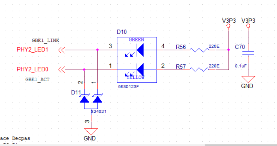
    • The "LED_GPIO_POLARITY" setting .it is through "strap pin configuration" or Register configuration(Address = 0X19).
    • my LED configuration is "Active low" in the design 
    • Autinagotiation - So i will change the Resistor in pin 47 to NL(No load ) in design  )
    • I have attached images of the LED section

    Regards

    Anees PK.

  • Hi Anees,

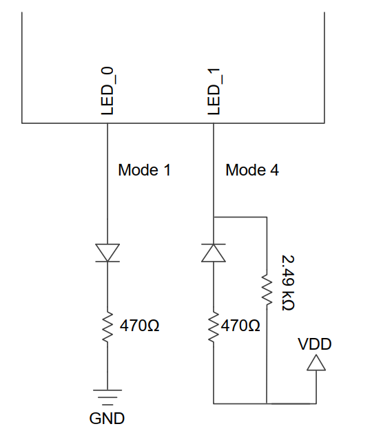
    LED polarity is mainly set through strap. In Figure 31 of section 9.5.2 of the datasheet, the strap (2.49K) for LED_1 is configured to be pulled high and the circuitry is configured to be an active low driver. In this scenario, you should not have to perform register writes, but I would double check the register (0x19) to ensure the polarity is set appropriately. Your configuration/circuitry seems to be the same, so you should be good.

    Regards,

    Adrian Kam

  • Hi Adrian,

    In the datasheet, the sample LED connection is given below. One is Logic low and the other is logic high.

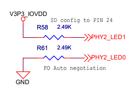
    In the schematic design, i have connected like  below 

    Please confirm the same whether we need to set the LED asper the datasheet or we can configure the same through register (0X19).

    Regards

    Anees PK.

  • Hi Anees,

    In your schematic, your LED1 configuration is the same as the logic high configuration in the datasheet. In this configuration, since the strap input is resistively pulled high, it will be an active low driver. If LED0 is also suppose to be active low, then your LED0 configuration should be the same as your LED1 configuration. The strap option should not matter since you are operating it in RGMII to 100FX mode, but pulling R61 high will configure the pin to be an active low driver. Doing this will not require you to perform register writes.

    If you decide to set R61 as "no connect", then you will need to write to register 0x19 to configure LED0 polarity.

    Regards,

    Adrian Kam

  • Hi Adrian,

    I understand the below.

    I have 2 options to for LED Active low configuration.

    Option 1 - Keep R61 resistor to pullup to IOVDD

    Option -2 - Keep the same resistor strap configuration and Set the resister 0X19.

    Please confirm the same.i have planed to Option-1

    Regards

    Anees PK 

  • Hi Anees,

    You are correct. I would also recommend going with option 1.

    Regards,

    Adrian Kam

  • Hi Adrian,,

    Thanks 

    Regards

    Anees PK.

  • Hi Adrian, 

    One more conformation-

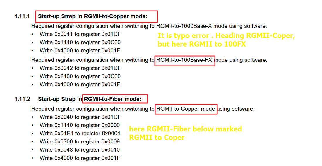
    As per the application note SNLA318 the strap table mentioned the pins are NL or Open, But in the datasheet connect to GND.

    Please confirm the resistor keep open  or Pulled Down 

    Application note

    Datasheet-

    Also please confirm it is typing issue -


  • Hi Anees,

    The strap can be keep open or pull down. If the strap is open, the default will be used.

    It is a typo issue. The bold headers are inaccurate. For clarity, here is the correct order of headings:

    1. RGMII to 1000Base-X
    2. RGMII to 100Base-FX
    3. RGMII to Copper

    Thanks for bringing this to attention, and we will work on getting this fixed in the app note.

    Regards,

    Adrian Kam

  • Hi Adrian Kam,

    Please share the following details related to the layout.

    • In design, we configured as RGMII to 100Fx,SGMII , so the RGMII signal frequency is 250MHz? and SGMII signal is 100Mhz?
    • RGMII signal required only 50Ohz impudence and length matching or need to do Signal integrity?. Datasheet mention only impudence and length matching for RGMII signal. Please confirm the same.  
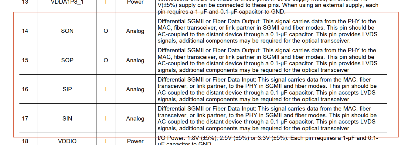
    • The datasheet mentions the  SON/SOP signal is Output, Also mention "Signal carriers data from PHY to the MAC".Please conform these signals are connected to Fiber - AFBR-5803AZ  TO(Transmit pin ) pins.

    Regards

    Anees PK.

  • Hi Anees,

    1. In RGMII to 100FX mode, RGMII clock should be 25 MHz. The clock frequency for SGMII is typically 625 MHz. 
    2. Along with 50ohm impedance and length matching, the following should be considered as well:
      1. Total length of the traces should be less than 6 in.
      2. Try to avoid crosstalk unless there is a GND layer to separate traces.
      3. Length matching should be done on mismatched ends.
    3. SON/SOP should be connected to the transmit pins.

    Regards,

    Adrian Kam