This thread has been locked.

If you have a related question, please click the "Ask a related question" button in the top right corner. The newly created question will be automatically linked to this question.

ISO3082: Isolated RS485 & Analog Input circuit ( ISO7320FCD )

Part Number: ISO3082
Other Parts Discussed in Thread: ISOW1412, ISO1410, ISO6740, ISOW7721, ISOW7741, ISO1212, ISO1211, ISO6720, AMC1351, SN6505B, ISOW1432, SN6505A, ISO1412, ISO1430, ISO1432, ISO1452, ISO1450

Hi Team,

Greeting!!

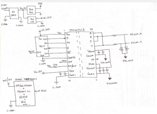
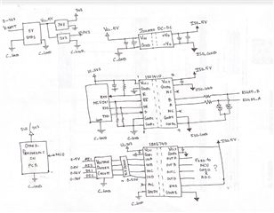
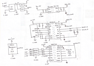
In our new application, we are going to design a signal & power isolated the RS485 ( 2 different channels ) section using ISO3082DWR and Isolated Analog inputs using  ISO7320FCD ( 2 channel )

Please find the list of queries below,

 Regarding ISO3082DWR :

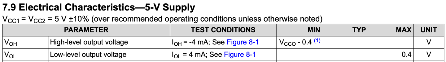
1. As per the datasheet, the maximum operating current of the Transceiver is 60 mA. Since we are going to use 2Nos of ISO3082DWR to achieve 2 channels RS485 the maximum supply current required will be 120mA. Is that correct? Our data rate requirement is 200kbps only.

2. What will be the current consumption of this part in idle mode?  10 uA?

3. we are planning to use an Isolated DC-DC converter with 200mA output to drive the above section. Hope this will be sufficient. Kindly advise here.

Regarding ISO7320FCD :

1. We need 2Nos of Isolated Analog input for our application. so we planned to use ISO7320FCD for the same. The input analog voltage which we want to detect will be in the range of 0 to 5V. hope this part will satisfy our requirement. Kindly clarify.

2. Idle/low power mode of this IC has a current consumption of 10uA. So if we keep the input open then current consumption won't go above 10uA is that my understanding correct?

  • Hi Nandha,

    Please find my replies

     Regarding ISO3082DWR :

    1. The maximum driver current is 60mA and Icc2 consumption is 15mA. So the total comes up to 75mA on right side per device, 2 devices will need 140mA. you can explore our newer parts like ISO1410 with better performance.
    2. Current consumption is idle mode is 8mA on ICC1 and 15mA on ICC2. The 10μA which you mentioned is for D, DE pins. 
    3. The DC-DC converter with 200mA should be sufficient but I would suggest you use our devices with integrated power which are optimized for the best performance like ISOW1412 

    Regarding ISO7320FCD 

    The ISO7320FCD is digital isolator and you have to use an ADC or comparator and the digital data can be fed through digital isolators. Please use our newest part ISO6720 for digital isolation.

    Hope I have answered your questions. 

    Thanks
    Vikas J

  • Hi Vikas,

    Noted with thanks!

    We reviewed all your points above and we have some more queries here as follows,

    Regarding RS485 Isolation ckt:

    Item1: Approach with ISOW1412 ( Integrated power & signal isolation )

    Here we would like to inform you one thing, Including RS485 ( 2 Ch ) we have some other peripherals also in our design like LTE/GPS modem, RS232, and BLE, etc., Here I have attached a schematic reference of our approach with ISOW1412, Please refer below

    1. Can we use the Input side GND plane ( C_GND ) for all other peripherals and power trees as shown in the above image?

    2. Current  ISOW1412  is out of stock in all vendor platforms. How about the availability of this part? Our requirement will be 40k/year with a project life cycle of 5 years. So we need clarity on the availability of this part. 

    3. Maximum operating current of our overall product is designed for 1 to 3 Amps max. Will this affect ISOX1412?

    4. Can we use the same power supply ( VCC_5V ) to both Vio and Vdd of this part?

      Item2: Approach with ISO1410

    Schematic reference

    1. In this also need to know where we want to connect all other peripherals. 

    2. Also with reference to the above image, We would like to use ISO6740 to have isolation for Analog input and Digital input circuits. On the input side, we have connected Analog input ( 0 to 5v ) and digital input ( 0 to 36v ) after the voltage divider ( output will be 0 to 3v3 to MUC ). We are expecting the same input voltage ( On INA to IND ) as the output voltage ( On OUTA to OUTB ), There will be any voltage drop on the IC side? 

    3. We need to read output voltage from OUT pins by MCU to measure input voltage. Hope there won't be any voltage drop on the isolator. Kindly confirm.

    4. As shown in the image. Can we connect the Output of ISO6740 to MUC which is there on the Input side of ISO1410? will that create any noise issues?

  • Hi Nandha,

    Thank you for considering out recommendations and for sharing additional inputs. Please allow me address your questions.

    ISOW1412:

    1. Can we use the Input side GND plane ( C_GND ) for all other peripherals and power trees as shown in the above image?

    Yes, GND1 of ISOW1412 needs to be connected to the system ground (C_GND) either directly or through ferrite beads (FB) for the device to be used. The device can operate normal in both use-cases but we recommend using FBs to optimize the design for low radiated emissions. Please follow the datasheet recommendations for how and where to use ferrite beads.

    2. Current  ISOW1412  is out of stock in all vendor platforms. How about the availability of this part? Our requirement will be 40k/year with a project life cycle of 5 years. So we need clarity on the availability of this part. 

    ISOW1412 is one of our latest and popular devices and is high in demand. The device gets stocked regularly and it also gets sold quickly due to high demand. I recommend that you subscribe to the part by clicking on "Notify me when available" button in the ordering section so that you get a notification email as soon as the stock becomes available.

    3. Maximum operating current of our overall product is designed for 1 to 3 Amps max. Will this affect ISOX1412?

    As stated in the datasheet, ISOW1412 requires a maximum input current of 292mA under worst-case test conditions. For your test conditions, you can refer to the datasheet to find out the max input current required. As long as the power supply powering ISOW1412 is supporting this current with some margin and sufficient decoupling capacitors (for peak currents) then we don't expect any issues. Please make sure ISOW1412 current consumption is budgeted into your product total current.

    4. Can we use the same power supply ( VCC_5V ) to both Vio and Vdd of this part?

    Yes, the two supply pins can have a common input supply or separate supply voltages. Please make sure the I/O logic signal levels match VIO supply voltage irrespective of what is connected to VDD.

    ISO1410:

    1. In this also need to know where we want to connect all other peripherals.

    The explanation from ISOW1412 holds true to the DC/DC converter in this case as well, especially if you are using ISOW7741 / ISOW7721 for the DC/DC conversion. If you are using a different device, we recommend that you refer to the respective datasheet for the guidelines and also may reach out to relevant E2E forum for reviewing your schematic.

    2. Also with reference to the above image, We would like to use ISO6740 to have isolation for Analog input and Digital input circuits. On the input side, we have connected Analog input ( 0 to 5v ) and digital input ( 0 to 36v ) after the voltage divider ( output will be 0 to 3v3 to MUC ). We are expecting the same input voltage ( On INA to IND ) as the output voltage ( On OUTA to OUTB ), There will be any voltage drop on the IC side?

    Not sure if I completely understand your use-case here. A 36V digital input when down-converted to <5V can be connected to ISO6740 without any issues and the output of ISO6740 will reflect the same logic at the output without any issues. The output voltage will depend on the supply connected to its respective VCC as stated in datasheet (see image below). As you can see, a HIGH output will be 4.6V minimum and LOW output will be 0.4V  maximum when its VCC is 5V.

    We also have a dedicated device for industrial digital inputs (24V) which integrates many features. Please refer to ISO1211 or ISO1212 for this.

    For the 5V analog input, ISO6740 is a digital isolator and it only accepts and outputs digital signals. If an analog signal is applied, the device will treat it like a digital signal and produce a digital output. Like I mentioned above, the output is going to be either 0.4V max for LOW or 4.6V minimum for HIGH, no intermediate voltage.
    Please refer to the below link that describes how a typical analog input module is designed. It also includes typical block diagram, device recommendations and many reference designs. You could choose the one that is most suitable for you. As described on this page, analog signals are applied to ADCs first to convert into digital data and then passed through digital isolators for isolation and then fed into an MCU through SPI, I2C or UART.

    https://www.ti.com/solution/analog-input-module

    We do also have isolated amplifiers that accept analog input signals and produce analog output signals. But these are typically used for special occasions and generally not for analog input modules or PLCs.

    https://www.ti.com/isolation/isolated-amplifiers/overview.html

    3. We need to read output voltage from OUT pins by MCU to measure input voltage. Hope there won't be any voltage drop on the isolator. Kindly confirm.

    As stated earlier, the output of ISO6740 is going to be digital with LOW/HIGH corresponding to 0.4V/4.6V and no intermediate voltage between 0.4V and 4.6V will be generated.

    4. As shown in the image. Can we connect the Output of ISO6740 to MUC which is there on the Input side of ISO1410? will that create any noise issues?

    Outputs of digital isolator can be connected to digital input pins of MCU, analog signals will need to be converted to digital and isolated or analog signals can be isolated using isolated amplifiers before connecting to ADC of MCU.

    I hope all the above inputs help you with clarity on how to proceed. Thanks.


    Regards,
    Koteshwar Rao

  • Hi Koteshwar Rao 

    Thanks for the explanation, Most of my queries were resolved. From your answer, I got below questions,

    1. Assume we are using GND1 of ISO1410 as a system GND of PCB ( for other peripherals ) as you said. Now MCU has system GND and Digital isolator ISO6720B which we used for Digital i/p isolation have Isolated GND ( GND2 ) on the output side. Can we give these outputs of ISO6720B to MUC directly? they have different GND potentials right? this won't affect

    Suggest if there is any better solution for isolated digital analog input applications. ( with analog input we need to calculate the voltage i.e, voltage sensing)

    2. In our design we have 2 DI & 2AI sections which all need to be isolated. since ISO6720 won't handle Analog input ( ADC ). Could you please suggest IC for analog input isolation ( 2 channels)? 

    Application: The analog input voltage will be 0 to 5V. we need to read this voltage by MCU after isolation. 

  • Hi Nandha,

    Thanks for sharing further inputs.

    1. I see that the MCU is on the left side of isolator sitting on system ground labelled C_GND. The outputs of digital isolator and RS-485 are all on the isolated ground labelled ISO_GND on the isolated side. The two sides (left and right) are isolated using digital isolator and they should only communicate through the isolator. If they are bypassing the isolator and getting connected directly to each other then there won't be any isolation between the two sides.
      1. If you meant to connect isolated outputs on the right side to another MCU on the right side, then there is no problem in doing so as the MCU on the right side is anyways going to be referenced to ISO_GND.
      2. Please also note that ISO6740 has two separate die in device with each having its own circuit referenced to its own ground (GND1 and GND2). These circuits operate independently, and if you short GND1 and GND2, the device will still work normal and will meet all electrical and switching parameters from datasheet. Since they are two independent circuits, it doesn't matter what ground they are connected to.
      3. To maintain isolation between the two circuits of ISO6740, the two grounds should be connected to the circuits on their respective side.
    2. Please note that it is not just ISO6720 but no digital isolator will be able to accept and produce analog inputs. To isolate an analog signal, you would require an analog isolated amplifier or a data acquisition system (Amplifier + ADC + Isolation).
      1. You may not have looked at the links I have shared earlier, these links have block diagrams of how an analog input and digital input modules look like, example device part numbers list for each block and many reference design examples (which include Schematic, PCB layout and test waveform of various DI and AI module designs).
        1. https://www.ti.com/solution/analog-input-module
        2. https://www.ti.com/isolation/isolated-amplifiers/overview.html
      2. I am sharing below a direct link to the block diagram listing device suggestions and associated reference designs.
        1. https://www.ti.com/solution/analog-input-module?variantid=14332&subsystemid=18085
      3. I am sharing below a couple direct links to the reference designs for analog input modules.
        1. https://www.ti.com/tool/TIPD164
        2. https://www.ti.com/tool/TIPD166
      4. I am listing below an X-Y matrix listing analog isolated amplifiers suggestions for current and voltage sensing from the link I shared earlier.

    I hope the above suggestions help me choose the best device for your application. If you any questions related to the analog isolated amplifiers, please create a new E2E post referring to the device of interest (like AMC1351) and the respective team will get back to you.

    Let me know if you have any other questions, thanks.


    Regards,
    Koteshwar Rao

  • Dear Team,

    Here I have attached the Final schematic of Our Isolated RS485 Section using ISO1410. 

    Kindly review and share your comments. 

    ISO1410-Review Sch.pdf

    Also, We hope the below parts are p2p compatible with ISO1410. Please confirm the same. 

    ISO1450DW

    ISO1452BDW

  • Hi Nandha,

    Thanks for sharing the schematic for review.

    The schematic looks good and i do not see any major concerns. Please make sure you follow the PCB layout guidelines from datasheet.

    For isolated power supply solution, we also have SN6505B / SN6505A that supports currents upto 1A. This is one of the most popular isolated power supply solution from TI. If you would an integrated solution and not use external transformer, then we also have isolated RS-485 transceiver with integrated DC/DC converter. We have two speed options for this, please check ISOW1412 and ISOW1432. They are pin-compatible to each other.

    Regarding your P2P question, please note that ISO14xx family has full-duplex devices and half-duplex devices. The two devices have different pin-out due to the topology itself, then they are not P2P. But the family has 3 half-duplex devices that are P2P to each other and 3 for full-duplex that are P2P as well. Half-duplex devices ISO1410, ISO1430 and ISO1450 and the basic isolation variants of these devices (with suffix 'B' in part number) are all P2P with a total of 6 devices that are P2P. Similarly, full-duplex devices ISO1412, ISO1432 and ISO1452 and their basic isolation variants are all P2P, this is another 6 devices.

    Please see below snapshot from datasheet listing all the variants and their differences. Thanks.


    Regards,
    Koteshwar Rao