


Other Parts Discussed in Thread: SN74HCS244
Hi Team,
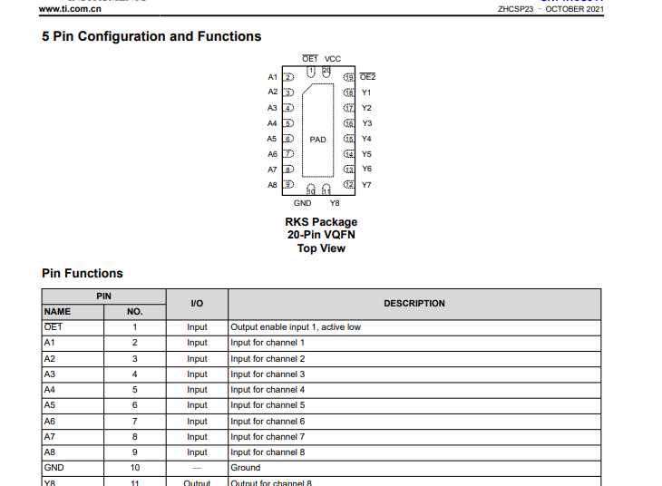
Could you tell me why the pin numbers and functions defined by the chip are different from those of the recommended layout?

Hi Team,
Could you tell me why the pin numbers and functions defined by the chip are different from those of the recommended layout?

