


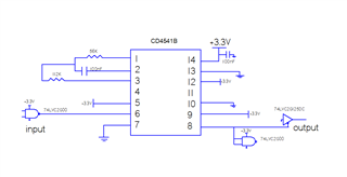
Part Number: CD4541B
Other Parts Discussed in Thread: SN74HC4060, CD74HC4060
We have implemented the component but we have some problems with it during our tests.
Configuration of the CD4541B :
Between pin 1 and 2: a Resistor and a capacitor R=56Kohm, C=100nF.
Pin 3: 120Kohm resistor connected to the middle of the C and R of pin 1/2.
Pin 4: NC
Pin 5: +3.3V
Pin 6: Connected to our Reset signal (output of a logic gate)
Pin 7: GND
Pin 8: Our output signal. Connected to the input of a logic gate
Pin 9: +3.3V
Pin 10: GND
Pin 11: NC
Pin 12: +3.3V
Pin 13: GND
Pin 14: +3.3V
At power supply increase (+3.3V) the output is activated during 1.6s. We do not understand why is activated because the MR pin is not activated. We have verified that there is no peak at this initial stage with the oscilloscope.
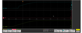
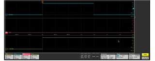
Could you please help us to understand why the output is activated at this initial stage of increase of the power supply?


