This thread has been locked.

If you have a related question, please click the "Ask a related question" button in the top right corner. The newly created question will be automatically linked to this question.

CD40109B: CD40109B for 3.3 V to 15 V Translation

Part Number: CD40109B
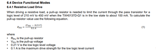
Other Parts Discussed in Thread: UCC44273, UCC27517, TXH0137D-Q1, CD4504B, TXH0137D,

This is reg translating a 3.3 V PWM Signal to +15 V levels with approx 5 mA Source & Sink 

CD4504 Data Sheet is not guaranteeing this translation .

Some one from TI ( in some earlier threads ) had recommended CD40109 with Vcc as 3.3 V and Vdd as 15 V 

and applying the 3.3 V DSP PWM Signals to the 3.3 V Side.

While studying the Data sheet of CD40109 , this Fig No 10, High Level Supply Voltage Vs Low Level Supply Voltage,

the recommended Domain is not a perfect Rectangle but the Left vertical line appears slanted.

Essentially for a 15 V  along the vertical axis, where this slanted line intersects and I drop it to the Horizontal axis 

does it guarantee 3.3 V , is my Question.

If I recall, ( though not sure ) even CD4504 has a similar slanted line.

Would someone be good enough to  clarify?

Thanks and regards

Varun

  • Each square is 0.5 V, so 3.3 V input is not recommended with 15 V output. (And the datasheet does not guarantee a drive strength of 5 mA.)

    Use a gate driver like the UCC27517/UCC44273.

  • Thanks for your reply.

    BR

    Varun

  • Hi Varun,

    You may also see TXH0137D-Q1, thanks.

    Best Regards,

    Michael.

  • Hi Mike

    Thanks for your mail & happy to interact with you.

    The problem with Open Drain / Open Collector Interface IC's

    lile TPL7407, ULN2003, and your suggested one ,TXH0137D-Q1 is that

    while they can sink a fairly large current, sourcing is limited by the

    Pull up Resistor and the voltage drop from the Vcc tolerable, when Hi.

    For example, you want to have a 15 V O/P with at least 12 V level when sourcing 5 mA.

    The Pull up resistor can be no more than 600 Ohms each.

    The reqd Pd for each Res ( cont Low ) would be 375 mW. the size of a 1 W Res

    would use lots of Board space

    UCC2752X Series would be more usable , however they provide only two Channels

    while generally Six channels are reqd

    Looks like a Trade off between Three such Gate driver IC's or two packages one

    to translate 3,3 V to 5 V and then CD4504B to translate to 15 V .

    What do you think ?

    BR

    Varun

  • Mike

    Just to point out a small mistake in the Product details for TXH0137D

    It shows ( giving the impression that it can Source & sink that 100 mA )

    IOH (max) (mA) 100

    IOL (max) (mA) 100

    Varun

  • Hi Varun,

    Yes, you may use the TXH recommendation for 3.3 V to 5 V or to 15 V.

    Your pull-up can also be more than 600 ohms as the device is recommended for up to 100 mA.

    Please help use equation 1 of the datasheet to help estimate your pull-up sizing for 5 mA -  3.3 V / 5 V / 15 V translation, thanks.

    Best Regards,

    Michael.

  • Hi Mike

    Thanks for your prompt replies

    Yes, you're right reg the Pull Up Resistors, albeit being bulky cinsuming Board space when 4 or 6 

    such translators are reqd, Gate Drivers would occupy less space.

    However, the Bottom line seems to be:

    1. One can't use CD4504B or CD40109B for direct translation of 3.3V to 15 V,

        as several Power Elex Engrs in my knowledge have tried to do 

        Pl check if I am right there?

    2. Gate Drivers , Dual or Quad from UCC275XX family are a better alternative.

    3. Earlier there was UDN Series Source Driver IC ( complement to ULN2003 type )

        somehow that went out of vogue, alas!!

    Thanks for your continued support, and I am closing this thread , pl have my above Q answered

    Thanks and have a grt day ahead

    Varun