


Other Parts Discussed in Thread: SN74LVC1G17, SN74LVC2G17
Hi All,
We are using SN74AUP1G74 as latch in my application, where we want to ensure Q# to be High post Power up of the IC. When we have fault, we use clock rising edge to pull Q# to LOW which in turn shuts off the system.
We have implemented an RC delay circuit at CLR# pin (2.2K, 1uF) to ensure output Q# to be in logic HIGH known initial state.
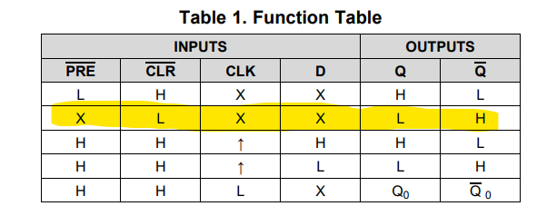
So, only during initial power up, CLR# pin has > 200 nsec/V Input transition rise rate and it stays high afterwards. Per figure 2 in appnote (https://www.ti.com/lit/ab/scea046a/scea046a.pdf?ts=1710996273842&ref_url=https%253A%252F%252Fwww.ti.com%252Fproduct%252FSN74AUP1G79) there seems to be an additional current draw during this instant. However, as this happens only once, we don't see any thermal issues. We ensured that we don't have any slow rising input at D and CLK pins. Please let us know if this is ok or do you see any issue?
Thanks
C.Pradeep

