This thread has been locked.

If you have a related question, please click the "Ask a related question" button in the top right corner. The newly created question will be automatically linked to this question.

LSF0108: QSPI signal two-way communication, when the rate increases to 50MHz, there is a problem of inconsistent data written and read

Part Number: LSF0108
Other Parts Discussed in Thread: TXB0106

hi ,

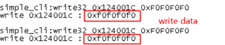
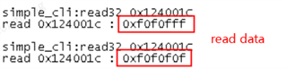
        LSF0108 is used for 1.2V and 3.3V level signal conversion for QSPI signal two-way communication. The target rate is 50MHz, but when the rate is increased to 50MHz, there will be inconsistent problems between the data written and the data read. At present, the measured maximum rate can only support the data and read data are consistent when the rate is 33.33MHz. Please also see what causes the inconsistency between the written data and read data when the rate is increased to 50MHz.

1. In the actual measurement, we have compared the pull-up resistance value in Table 9-3 of the data sheet, and learned that the speed of the pull-up resistance is too large to reach 50MHz, so we confirmed the pull-up resistance as 330Ω. When the pull-up resistance is adjusted slightly, such as 220Ω, there will also be inconsistencies between the written data and the read data when the speed is increased to 50MHz, which is verified by our actual measurement.

2. The measured link capacity load is below 30pF (about 20pF). According to the description in the data sheet, it should be able to reach 100-MHz, but now it has not reached 50MHz.

        Please also help to analyze what causes this. If you also have customers who have encountered similar situations, how to solve them? The board using LSF0108 has been returned to the board, and the packaging is inconsistent, so it is not possible to directly replace other devices such as TXB0801 for verification.

        Looking forward to your reply soon, thank you!

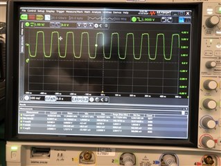
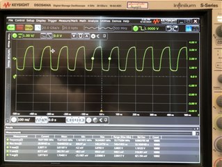
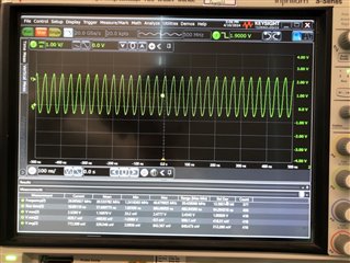
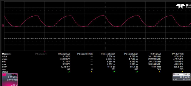
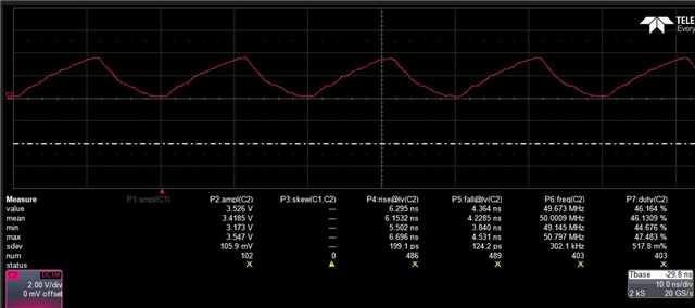
At 50MHz, there is an inconsistency between the data written and the data read, as shown in the following figure:

  • Please show an oscilloscope trace of the input and output.

  • I don't know why the upload of the waveform image is not successful. Please see the output waveform of CLK and DQ0 when 33.33MHz is uploaded in the previous post.

    https://e2echina.ti.com/support/logic/f/logic-forum/807520/lsf0108-50mhz?tisearch=e2e-sitesearch&keymatch=%20user%3A138085#

  • Hi Dongdong,

    Do you also have waveforms for the 50 MHz concern? I suspect that the pull-ups are too strong making the VOL too high for the observed inconsistencies.

    Please try gradually increasing pull-up size to find a balance for the data rate and VOL to help avoid concerned inconsistencies.

    You may also see Up Translation with the LSF Family further clarifying, thanks.

    Best Regards,

    Michael.

  • Waveform of CLK on the A-side at 50MHz:

    The waveform capture of DQ0 on side A at 50MHz is incomplete.

    Waveform of DQ0 on side B at 50MHz:

    At present, there is no pull-up on the A side, the default drive, the pull-up on the B side has tried to increase, tried 330Ω, 470Ω and 1000Ω, but there is no improvement. In fact, when the pull-up resistance is 470Ω, the driving ability is only about 7mA.

  • Hi Dongdong,

    Please note that schematic is not shown and unsure of DQ0. However, could you help clarify what is meant by incomplete? Why is the waveform amplitude 1.8 V when VrefA is 1.2 V? No pull-ups to 1.8 V? Also note that pull-ups are recommended with low sides experiencing signal integrity issues.

    For the B-side, could you help disconnect any peripheral connected to the B-ports and verify issue persists? Thanks. 

    Best Regards,

    Michael. 

  • hi Michael,

    1、DQ0 is connected to channel 5 in the schematic diagram, that is, A5/B5. Incomplete means that there is basically no available waveform measured. At 50MHz, CLK can still capture the available waveform, and DQ0 has not captured the available waveform。

    2、We need to use the existing EVB to verify the circuit. The existing EVB uses LSF0108 for 1.8V and 3.3V level conversion, so the A side is 1.8V, which I don't think will affect the verification conclusion. We have corresponding pull-up resistors on the AB side, and the comparison test results were the same. Later, the pull-up resistor on the A side was removed from the inside, because the IO on the chip side is in the PP mode.

    3、We did a verification today to remove the B-side peripheral and the test result is the same as before, no improvement.

    4、An experiment was done to verify that all the peripherals of all channels on the AB side were disconnected, and the CLK channel on the A side, that is, A4, was connected to the external signal generator using the coaxial line, and the signal generator was used to emit square waves, and the corresponding channel on the B side was measured using an oscilloscope:

    A-side waveform:10MHz

    B-side waveform:10MHz

    B-side waveform:30MHz

    It can be seen from the above waveform that the waveform after LSF0108 at 30MHz has been seriously deformed. Of course, the flying line verification has a certain impact on the signal integrity, but if the real use is similar to this, it cannot achieve good integrity. Please help to see whether LSF0108 really reaches 50MHz, thank you!

  • Hi Dongdong,

    t can be seen from the above waveform that the waveform after LSF0108 at 30MHz has been seriously deformed. Of course, the flying line verification has a certain impact on the signal integrity, but if the real use is similar to this, it cannot achieve good integrity. Please help to see whether LSF0108 really reaches 50MHz

    Similar to the referenced video, please note note that strong pull-ups are needed. Could you help double confirm the pull-up used for the shown 50 MHz waveform with all peripherals disconnected?

    Best Regards,

    Michael.

  • hi Michael,

    The actual measurement can not reach 50MHz, the waveform has been deformed at this time, and the waveform is basically consistent with 30MHz. According to the recommendation of the specification, the strong drive pull-up is added.

  • Hi Dongdong,

    Apologies for the typo. I meant the shown 30 MHz waveform. 

    B-side waveform:30MHz

    Are you indicating this is with strong pull-ups up to 330 ohms and no load similar to the video?

    Best Regards,

    Michael.

  • hi  Michael,

    Yes, this is the strong pull-up no load waveform.

  • Hi Dongdong,

    Thanks for confirming. Please see below for 30 MHz and 50 MHz with 330 ohms pull-up on both sides and would further recommend TXB0106 for QSPI applications if any concerns, thanks.

    Best Regards,

    Michael.