Good morning,
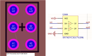
I am designing the library component for SN74LVC2G17, and I would like to double check the footprint for YZP package (DSBGA (6) )
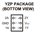
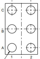
The manual shows the pin numbers as 1, 2, 3, 4, 5, 6. The usual convention for DSBGA packages is to use A1, A2, B1, B2, C1, C2.
https://www.ti.com/lit/ds/symlink/sn74lvc2g17.pdf
May I just double check that my assumptions are correct, namely
pin 1 maps to A1
pin 2 maps to B1
pin 3 maps to C1
pin 4 maps to C2
pin 5 maps to B2
pin 6 maps to A2
so the resulting pin is like the attached image?
Thank you in advance for the help.