Hello,
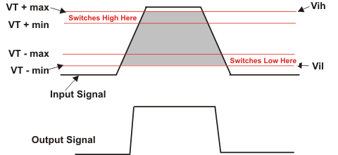
This is my first post here. I'm designing in the SN54SC6T17-SEP and I'm trying to calculate the DC level margins at the inputs to the device. I'm used to a table showing VIH(min) and VIL(max) for a particular range of VDD. The SN54SC6T17-SEP data sheet helpfully provides Figure 7-2 SCxT Input Voltage Levels. As I understand it, VIH(min) is represented by the red dashed line and VIL(max) is represented by the black dashed line. Does TI have a document with those two curves in tabular form or fitted equations in which I can enter VDD and temperature and get the VIH(min) and VIL(max) values? Section 7.3.4 says "Figure 7-2 shows the typical VIH and VIL levels ..." Are these curves available across temperature?
For example, let's say I want to know VIH(min) and VIL(max) at different VDD values:
- VDD = 4.75 and 5.25 V, Temp = -40 to +85 C
- VDD = 3.15 and 3.45 V, Temp = -40 to +85 C
- VDD = 2.45 and 2.55 V, Temp = -40 to +85 C
Thanks,
Rob