This thread has been locked.

If you have a related question, please click the "Ask a related question" button in the top right corner. The newly created question will be automatically linked to this question.

TXV0106: More datasheet issues.

Part Number: TXV0106

In addition to the error with the diagram on the first page of the datasheet, we have also found the following potential sources of confusion:

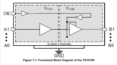
1. Figure 7-1 Functional Block Diagram of the TXV0106 shows an active high OE pin, as well as two internal invertors, the Output Enable should be active low right?

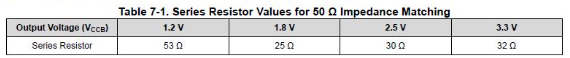
2. Table 7-1 Series Resistor Values for 50ohm Impedance Matching shows a 53ohm resistor for a 1V2 output voltage, this looks to be incorrect if you consider the resistor values given for the other output voltages 1V8, 2V5 and 3V3. Can you confirm the resistor value required for a 1V2 output? 

Thanks in advance

Nick

  • Hi Nick,

    You are correct and have followed up internally to help update.
    Please also note that the resistor value is not absolute but a recommendation per system designer’s acceptable tolerance levels. Hence, 20 ohms would also work, thanks. 

    Best Regards,

    Michael. 

  • 1. The TXV devices indeed have an active-low /OE input (and section 7.4 is correct). Apparently, the image was copied from a TXU datasheet.

    2. At 1.2 V, the typical output impedance is 0.1 V / 3 mA = 33.3 Ω, so the resistor value would be about 17 Ω.

  • Hi Nick,

    In addition to Clemens' feedback, please note that the 0.1 V is for NMOS driving LOW. PMOS driving HIGH would have a different output impedance i.e. MOS resistance increases significantly with 1.2 V and would recommend up to datasheet's 53 ohms as a balance. Meaning 53 ohms will not negatively impact driving both HIGH and LOW but 17 ohms may help with LOW but not significant enough when driving HIGH.

    Hence, best to adjust with different values as you deem fit per your system requirements, thanks.

    Best Regards,

    Michael.