SN74LVC1G74: SN74LVC1G74 - latching time

Part Number: SN74LVC1G74
Other Parts Discussed in Thread: TPS3422, SN74LVC1G123

Tool/software:

Hi ti team,

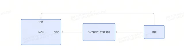
Please check the design of the latch. The requirement is that after triggering MCU to wake up, the low level state of the key press should be kept for about 1S, and then the GPIO of MCU will read it.

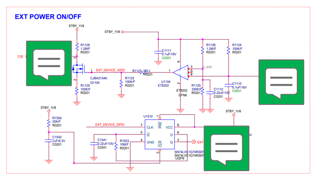
1. Help to check the peripheral schematic design of SN74LVC1G74RSER.
2. As shown in the following figure, which formula is used for the latching time?

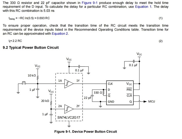
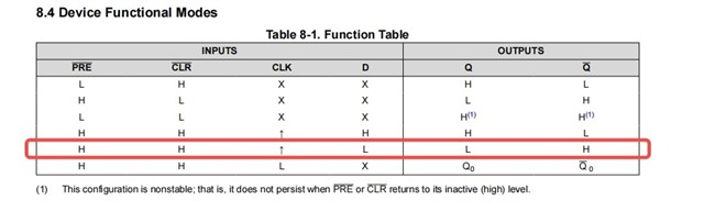
3. As shown in the figure below, both PRE and CLR are set high. When CLK detects the rising edge, Q outputs a low level, which is the result I want. (not added RC circuit); And then after latching 1S (according to RC), Q gets higher, right?

  • This circuit does not have a one-second delay. (The hold time is only 5 ns and refers to something different.)

    Your specification is unclear. What should happen to the output when the button is pressed? What should happen to the output when the button is released? Is there a difference when the button is pressed for shorter or longer than 1 s?

    You probably want a push-button controller like the TPS3422 (which has a delay of 7.5 s).

  • Hi Clemes,

    1, my demand is that when the key is not pressed, the output high level, when the key is pressed, the output low level, and keep for about 1s, and then restore to the default high level.

    2. My application scenario is as follows: When the key is pressed, the interrupt response will trigger the MCU to start up. After more than 400ms, the MCU will start up, and then read the GPIO status to identify it as a key, so SN74LVC1G74RSER needs to press the key state (low level) for about 1S to GPIO. After MCU is powered on, read the GPIO status and perform the next software operation.

    3.Please check the schematic.

  • The SN74LVC1G123 does output a fixed-length pulse, but the pulse is high, not low. If you cannot change the software, add an inverter.