
- Ask a related questionWhat is a related question?A related question is a question created from another question. When the related question is created, it will be automatically linked to the original question.
Tool/software:
Hello
We have such a issue. LDAC signals have a lot of clutter signals during each cold boot from -5℃ before FPGA loading complete . It will cause the DAC work abnormal.
LDAC is always high at room temperature. the issue can't be reproduce at room temperature.
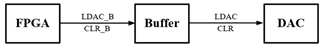
Our design block is like this:
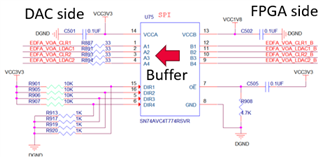
Here is our circuit:
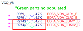
The pull up resistor of LDAC_B is not populated at BOM.
If we populate the pull up resistor of LDAC_B, issue can't be reproduce at -5℃.
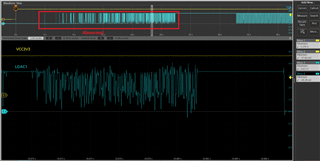
Here are abnormal waveform:
Can you help to explain why this issue happens at low temperatures and not at room or high temperatures?


