


Other Parts Discussed in Thread: SN74AXC2T245
Tool/software:
Hello,
I am using a SN74AVC2T245RSWR for low-delay voltage translation. I would like to know what the behavior of output B is given the following diagram (the waveform section I am interested in is highlighted as a question mark with purple):
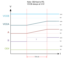
From the datasheet, I can see the propagation delay values at fixed voltage levels given to VCCA and VCCB, but I do not see what the behavior of B is if the OE# pin is always activated and both the voltage ramps to feed VCCA and the A input go high at the same time.
Can somebody provide an input on this?
Thank you.

