Other Parts Discussed in Thread: TPS38700
Tool/software:
Hi Everyone,
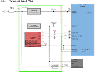
I am looking for DC-DC converter or a solution to match power-up sequence between Artix-7 FPGA and SN74VMEH22501A with live insertion capability.
Below are the sequence for FPGA and SN74VMEH22501A
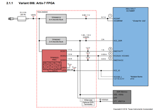
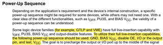
Power-Up Sequence for XC7A100T FPGA
-
Power Supply Initialization:
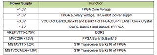
- VCCINT (Core Voltage): Typically 0.95V. This is the internal core voltage that powers the FPGA's logic and internal circuitry.
- VCCO (I/O Bank Voltage): Depends on the I/O bank. Common voltages are 1.8V, 2.5V, or 3.3V. This powers the I/O banks and should match the required voltage level for the specific I/O configuration.
- VCCAUX (Auxiliary Voltage): Typically 2.5V or 3.3V. This supplies power to auxiliary functions, including the configuration logic.
- VCCBRAM (BRAM Power): Typically the same as VCCINT, around 0.95V, as it powers the Block RAMs.
Recommended Sequence and Ramp Rates:
- Apply VCCINT and VCCBRAM first, as these are critical for the core functionality.
- Next, apply VCCAUX to power the auxiliary circuits.
- Finally, apply VCCO to power the I/O banks. Ensure that the I/O voltage is stable before connecting to external peripherals.
Ramp Rates:
- Voltage ramp rates and settling times should be in accordance with the FPGA's datasheet. Typically, ramp rates of 50-100 mV/ms are used to avoid overshoot and ensure stable power.
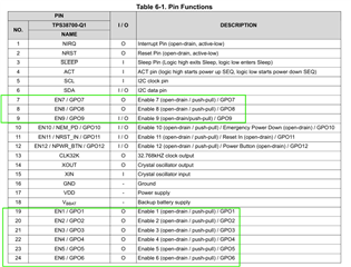
- Power-up sequence for SN74VMEH22501A
Please help me to create Power sequencing subsystem using TI product line.
Thanks,
Gaurav