This thread has been locked.
If you have a related question, please click the "Ask a related question" button in the top right corner. The newly created question will be automatically linked to this question.
Dear Sirs
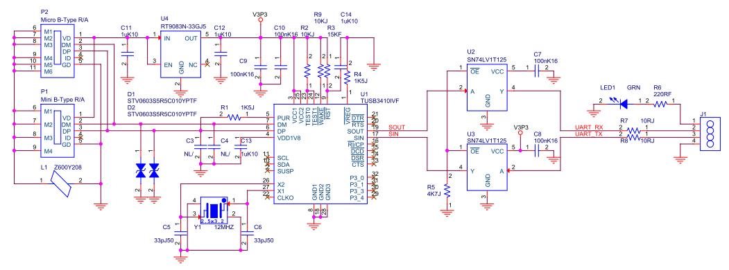
I need your help to confirm the SN74LV1T125 design. Thanks.
U2.A: UART Output(3.3V level)
U2.Y: UART Output via level shifter(1.8V level)
DUT Tx & Rx has a 1.8V level signal already (connected by J1)
We do not supply the VCC for U2 and U3 (SN74LV1T125 ).
1.Why connect to our DUT (by J1), U2.VCC will has a fixed 3.3V or 1.8V power on it ?
2. Could you provide the internal structure of SN74LV1T125 for VCC and Y?
Thanks
BRS
Nat
Hi Nat ,
In the schematic , the U2 Vcc is not powered up ? Basically , SOUT and UART_Rx will be isolated and Rx should be floating . U2 should be powered up to 1.8Vcc to have 3.3V SOUT to 1.8V level .
1) I couldn't understand your query precisely , please elaborate .
2) I don't have the access to the internal structure of the device , although I can provide you the functional block diagram .