This thread has been locked.

If you have a related question, please click the "Ask a related question" button in the top right corner. The newly created question will be automatically linked to this question.

SN74AUP2G00: Reset dominant SR latch

Part Number: SN74AUP2G00
Other Parts Discussed in Thread: SN74HC00, SN74AUP2G17

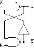
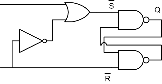
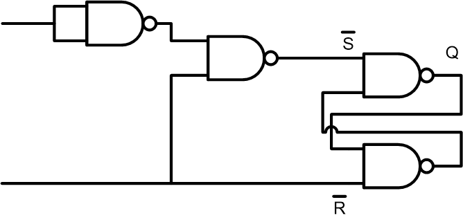
I am using the SN74AUP2G00 to make an active low, SR latch. How do I make the SR latch reset dominant? 

  • Hi Pradeep,

    The first result for this question on google has a pretty decent answer: https://electronics.stackexchange.com/questions/64831/given-a-gated-sr-latch-how-do-i-make-it-a-set-dominant-gated-sr-latch

    I think you could also do this instead, depending on your exact definition of "reset dominant":

    This just adds a little delay in the reset feedback loop, so if S\ and R\ are asserted at the same time, then released at the same time, the output should settle on Q = L and Q\ = H.  I think it's possible that this could also turn into an oscillator under the right conditions (I haven't been able to get it to happen in simulation though); the more complex solution linked above is probably the better bet.

    Here's a simulation of the above circuit:

    As long as the buffer is faster than the NAND gates, then it should prevent oscillation from occurring. You can see above that the Q\ output tries to switch low, but it isn't fast enough to fully switch, and the output returns high. Lighter loads produce even less of a glitch in the output.

  • Hi Emrys,

    Thanks for the prompt reply. I also saw that link but it didn't quite have what I was looking for. I did a little more tinkering and came up with this circuit. The OR gate will drive S\ high whenever R\ is low. This should make it Reset dominant, right? Any issues you see with it? Thanks!

  • Hi Emrys,

    I did some further simplification using just NAND gates and I want to see if you concur. The OR circuit can be constructed with NAND gates, right? Then the circuit would look like this:

    This can be further simplified to this by removing the redundant, cascaded inverter stages. Do you agree this should work? I'd like to just use NAND gates if I can.

  • Hey Pradeep,
    Yes, to all of the above. The first circuit does what you think it should, and the following two are correct conversions to NAND logic.

    Is there a reason you're wanting to only use NAND gates? The solution I showed would be smaller and simpler with less total delay. You could do this whole thing with just a single SN74HC00 (or any of the '00 quad NAND gate devices), but they would be much larger and use more power than the SN74AUP2G00 + SN74AUP2G17 solution, or even the 2x SN74AUP2G00 solution.
  • Hi Emrys,

    Thanks for the feedback and checking my logic.

    I think I'd rather use one chip (or type of chip) rather than having additional different logic chips. I like your idea of using a single SN74HC00. I also want to make sure that reset always dominates set. The logic makes more sense and appears more robust to me than using the feedback delay you first suggested.

    Thanks!