A related question is a question created from another question. When the related question is created, it will be automatically linked to the original question.
If you have a related question, please click the "Ask a related question" button in the top right corner. The newly created question will be automatically linked to this question.
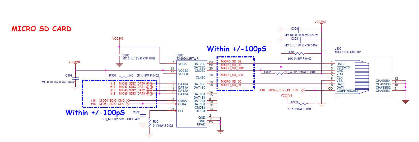
In the above schematic, I see you plan on supplying the SD Card with 3.3V. If this is the case, then VCCB0 will also need to be connected to this same source (VCC3V3).
Other than that, I don't see any problems with your design.
Please don't hesitate to post back with any other questions.