This thread has been locked.
If you have a related question, please click the "Ask a related question" button in the top right corner. The newly created question will be automatically linked to this question.
Hi
We are using TI Parts as attached.
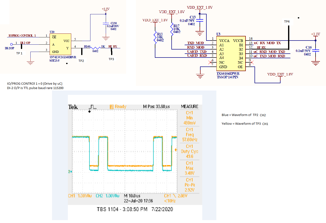
PN1:- TXS0104EPWR
PN2: SN74LVC1G240DBVR
we transmit TTL pulse of 115200 baud rate from DI-2 OP and observe the waveform at pin 12 of u3 (TXS0104EPWR) that singal clipped at low side, at low it goes to 480mv. and the datasheet of U3 said low level input voltage is 0.15V (max).
Q1) why its go to 0.480V loe levell, ideally U3 has interal pull up of (10K), so low level should be 3.3V/(1K+10) * 1K =0.3V but still going out of spec.
Q2) I tried to make R160 ohm , and low level comes to Zero volt.
Q3) can we make R160 value to O ohm in this application, does buffer SN74LVC1G240DBVR really require output resitor (1K).
Q4) or in worst case can we make R160 value to lower side like 250E.
The listed VIL value is not really a requirement; it is listed only because VOL depends on it: the output voltage is the input voltage plus the voltage drop over the switch.
What is the original purpose of R160? If there is a long trace between U20 and U3, then it should be no larger than the characteristic impedance of the trace, which is probably about 100 Ω.
Hi
Track length between U20 and U3 is around around 100 mm.
Design was taken form old referecne , not sure why R160 used , to limi the current of SN74LVC1G240DBVR or else. That why asking can we replace the R160 with 0 ohm or some low like 100-300ohm.
so what is the VIL requiremnt of TXS0104EPWR.
also why its go to 0.480V low level(See figure given earlier), ideally U3 has interal pull up of (10K), so low level should be 3.3V/(1K+10) * 1K =0.3V but still going out of spec.
Please note that the current from both pull-up resistors flows through R160.
I cannot tell you what the original circuit designer thought. But I suspect that the resistor was intended to prevent overshoots due to the LVC's fast output edges. 100 Ω should work fine. (To have 0 Ω for DC signals but prevent fast edges, replace it with a ferrite bead. But that is probably too expensive.)
Strictly speaking, the TXS does not have a VIL requirement. If you increase the input voltage, the output voltage increases by the same amount. Only at input voltages higher than about VCCA − 1 V does the switch close.
so if TXS does not have VIL requirement than how it will indentified high and low level of incoming signal. in my curretn case high level is 3.3V an dlow level is araound 0.48V , so TXS can switch properly.
is there any reliability issue.
As I said, voltages higher than about VCCA − 1 V close the switch and result in a high output.
The TXS does not "identify" low signals; when the switch is on, the output voltage is the input voltage plus a small offset.