This thread has been locked.
If you have a related question, please click the "Ask a related question" button in the top right corner. The newly created question will be automatically linked to this question.
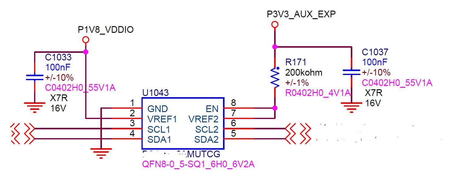
In a standard application, VREF_B and EN are tied together and connected to 3.3V through 200K resistor. VREF_A is 1.8V.
We have reworked a board to have above implementation. I observed a behavior where a GPIO signal connecting to the LSF0108 buffer Vref_A side and we measured the signal at VREF_B side is 1.8v, not 3.3V (there is a 2.2K pullup to 3.3V).
Question, if the GPIO is push-pull at VREF_A side, do we expect the signal is 1.8V at VREF_B side? This is because the Vbias is Vref_A + Vth, the SW FET should be fully ON? Is this the case for LSF0108 work as push-pull application?
Hi Ronnie,
No, the output is expected to be at VREF_B -- after ~5*R*C.
When one of the inputs (A or B side) is forced to 1.8V (VREF_A) with the appropriate bias circuit, as you described at the start, then the MOSFET is very close to OFF: V_GS = V_G - V_S = 1.8 + Vth - 1.8 = Vth -- ie there is not much overdrive voltage (only enough to drive ~6 uA of current).
This is the normal operating state for the LSF family of devices -- once the input is approximately equal to VREF_A, then the output is controlled by the pull-up resistor and load capacitance.
The most likely case here is that the signal is too fast for the given RC values and the output appears to stay at 1.8V because it doesn't have time to charge up to 3.3V. Reducing the pull-up resistor value to 330 ohms would be one way to check if this is correct.
Follow up question –
Hi Ronnie,
It's not quite as simple as you're making it out to be -- if the threshold is met the MOSFET is technically "ON" but it will supply no current if the voltage is _exactly_ the threshold. You must have an overdrive voltage to provide output current (ie voltage above the threshold value).
I hate to use first order MOSFET equations since they are not very good at representing real devices, but we can use them in this case. Recall the drain current equation for the saturation region (V_DS > V_GS - V_TH) -- in this case, V_GS -V_TH ~= 0, and V_DS should at least start larger than 0, so this is the best equation to work with.
I_DS = 1/2*u_n*C_ox*W/L*(V_GS-V_TH)^2(1+lambda*V_DS)
To simplify, replacing the constant parts with 'k' and removing the V_DS dependency factor:
I_DS = k*(V_GS-V_TH)^2
In our bias circuit V_GS = 2.6 - 1.8 = 0.8V
And our current is (3.3 - 2.6)/200k = 3.5uA
So we know that k*(0.8 - V_TH)^2 = 3.5 uA
We can then look at one of the channels and see that the exact same math applies.
When the gate is 2.6V (per your measurement), and the input is 1.8V, then we know that V_GS = V_G - V_S = 2.6 - 1.8 = 0.8V
We end up with the equation:
I_DS = k*(0.8 - V_TH)^2
Considering that k and V_TH haven't changed from the previous equation, we know that I_DS is still expected to be 3.5 uA.
To answer your questions directly:
Ronnie Hughes said:1. What is internal Vbias MOSFET VGS? We measured the Vbias is 2.6V. So the gate is 2.6V, according to TI datasheet description, if Vref_A rise up to 1.8V, the MOSFET will be OFF. And Vref_B will be pullup to 3.3V.
It varies from device to device, and is irrelevant to the solution (as shown above). The self-bias circuit eliminates the need for knowing this value -- which is great, since it changes under different circumstances.
Ronnie Hughes said:2. If the MOSFET is not OFF (but ON, if Vgs =0.8V), the voltage at Vref_B side will be clamped to Vref_A because the FET is ON. Is this a case?
No - a MOSFET is a voltage controlled current source - it cannot provide infinite current to clamp the output regardless of the control voltage. The control voltage must be relatively large to put the device into saturation and produce the effect you describe.
Ronnie Hughes said:3. For MOSFET, is the drain tied to VREF_B, not VREF_A?
No, this is a 4-port device. The source is always the lower voltage between channel A or channel B. The body is connected to GND.
You can learn more about this in the video series located here: https://training.ti.com/node/1139264?context=1139264
Customer has another question:
I have another question related to LSF010x isolation buffer.
There is an application where if the VREF_B is tied to 3.3Vaux (standby power), but Vref_A is 1.8V (main). When the system is OFF. So the Vref_A is 0V, but Vref_B is still 3.3V.
We see there is leakage to Vref_A which is on 1.8V rail.
Is this expected behavior?
Hey Ronnie,
I assume there are pull-up resistors for both sides of the SDA and SCL lines that are not visible - because it won't work without those.
The reason you're seeing leakage to the VREF1 pin is because that's how the device is designed -- when VREF2 & EN > VREF1 + 0.5V, then the bias circuit conducts. There's a video that shows exactly how this works here: Understanding the Bias Circuit for the LSF Family
If you want to shut off the device, I have a video that discusses exactly how to do that here: Using the Enable Pin with the LSF Family
It looks like you're using a PCA9306 - which does work exactly like the LSF010x family. I'm just curious, why didn't you include that part number in the post? That device is actually handled by a different team (I2C), which is why I'm asking. I certainly don't mind helping, but I find it odd to mislead us on this.