This thread has been locked.

If you have a related question, please click the "Ask a related question" button in the top right corner. The newly created question will be automatically linked to this question.

SN74LVC1G99: SN74LVC1G99- data sheet functions

Part Number: SN74LVC1G99

Hello

Need some help here of Digital Logic 101 ...

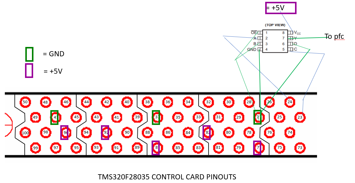
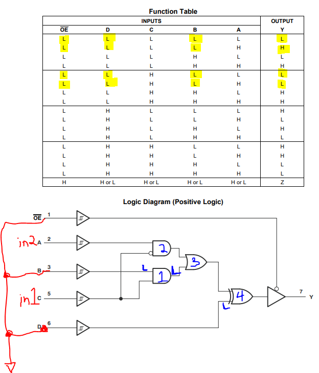
Trying to implement NOR with SN74LVC1G99 logic.

sing to hook up A,B,C,D but of course not getting NOR function on inputs. The chip is ignoring Pin5 input. On top of that, not doing inversion of NOR.

From Page 5, our selection is as given in the attached ppt. We are assuming inputs do not really have an order to drive into A & C

What are we doing wrong in this?

Any help will be highly appreciated.

r

74lvc1g99_hookup.pptx

  • Hi r,

    I have a feeling that this isn't what you intended to show me exactly, but this is how PowerPoint displayed your file for me:

    I don't think it really matters for me to know how the device connects to your connector though to help.

    -----

    We can check the function you've selected at the main function table for the device:

    Your PowerPoint indicated that you're trying to get a NOR gate with one inverted input.  Above I hooked up that function to the functional block diagram, and we can check how it works with the shown gates (I numbered them for easy identification).

    Gate 1 will always output LOW because one input is forced LOW (B), so we don't have to worry about that gate. (LOW AND anything = LOW)

    Gate 2 is an AND gate with one inverted input, so we can write the logic equation for it as: A * C\

    Gates 3 and 4 will act like buffers (Y = A) because one input is permanently LOW.  So really, our whole logic equation is just A * C\.  You can use DeMorgan's theorem to swap that to an OR function by doing the inversion of both sides:

    (A*C\)\ = (Y)\

    A\ + C = Y\

    or Y = (A\ + C)\

    AKA the logic equation for a NOR gate with one inverted input (pin A).  All we've done is verify that the functional diagram agrees with the other part of the datasheet. We can also double check the logic table, but I can say that it also agrees.

    -----

    The next obvious question is -- why isn't it working for you?  To answer this, I'd have to see your inputs and output - preferably with a scope shot including all of them together.

    I'd recommend to check the voltage at each pin of the device (not at the connector, but at the actual IC) to see if they have the expected inputs. I'd also check that the output isn't shorted to anything, as that can prevent it from changing states.

    I highlighted the part of the function table that's being used above, which I'll repeat here for clarity:

    C A Y
    L L L
    L H H
    H L L
    H H L

    The device should respond to the inputs above for A and C with the output of Y.  I'm assuming that you have OE, B, and D all tied to GND. Let me know if I can be of further help.

  • Emrys

    Thnx a lot for the effort you did on our question.

    Yeah, I followed the Logic you derived. But that is not what we wanted.

    Our goal is to get (A+B)/ , NOR

    The connection I did was following the datasheet  NOR connection. At least so I figured out from Page 5.

    Indeed, it seems to me that I did not interpret the Table in Page 5 correctly: because I do not understand how to interpret that table!

    The fact that output does not follow the input combo maybe due to many things- we are looking into it.

    BUT I am sure the connection we did following the ds suggestion is not going to give you (A+B)/

    What will?

    What if we wanted to try NAND function on A & B?

    That will be (A/+B/)

    How do we read the Table in ds to get this implemented?

  • The fourth table on page 5 says that to get a NOR gate, you have to connect the B and D inputs to a high-level voltage. In your graphic, B and D are connected to GND, which is a low-level voltage. This corresponds to the first entry in the second table on page 5, which is an AND gate with one inverted input. You must connect B and D to VCC instead.

    L = GND, H = VCC.

    To get a NAND gate, see the first table on page 6.

  • Emrys

    Correct! Got it...thnx much.

    closing this post

    r