This thread has been locked.

If you have a related question, please click the "Ask a related question" button in the top right corner. The newly created question will be automatically linked to this question.

SN74AUC1G125: Question about xOE fall-time requirement

Part Number: SN74AUC1G125
Other Parts Discussed in Thread: SN74LVC1G125,

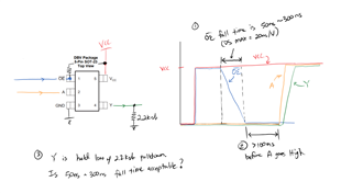
Below I attached an image of a use-case for the SN74AUC1G125 and SN74LVC1G125.

Basically, the datasheet states Δt/Δv is 20ns(max) when VCC = 1.5V, and 10ns(max) when VCC = 1.8V.

1) This goes for the xOE as well, right?

2) If the fall time to bring xOE LOW and activate the device is too long (50ns~300ns), then the output could flip back and forth between Hi-Z and driven, right?

3) For #2 above, what if A was LOW, and Y was pulled LOW via 2.2kΩ resistor, until >100ms after xOE was pulled low?
In this case, even if the output flips back and forth between Hi-Z and driven, it will still be LOW, right?
Is this an "allowable" violation of the Δt/Δv max limitation - since the output can only be LOW during the xOE fall transition?

  • This limit applies to all inputs, including OE.

    When the edges are too slow, the output could oscillate (which might not matter for you), but the device might also not work correctly, or get damages; see [FAQ] How does a slow or floating input affect a CMOS device?

  • Clemens,

    I read the article. I forgot about the shoot through current....

    im understanding that the H/L oscillations won’t be the issue for this application, instead it will be the shoot through current.

     the max Time in the DS is in the recommended operating conditions section, not the abs max.

    assuming VCc=1.8V, worst case is you have a connection to VCC and GND Via Mosfets for <600ns.

    Offline, is there any way to do a thermal simulation and see if this is enough to heat up and damage the cmos transistors or bond wires?

    i am assuming the DS recommended value relates to the max time to avoid output oscillations, but that it does not relate to the Shoot through current limitation of the device.

    RDs(on) is worst case current...if say 5Ohms, we are talking about a worst case instantaneous current of 360mA. 

    Darren

  • Hey Darren,

    At 1.8V supply, there won't be any concern with damaging the device with a 50 to 300ns transition at the input. You will see increased power consumption, but even the output drivers on LVC won't be able to pull enough current at that voltage to exceed the device's maximum limits.

    The bigger concern is with those internal oscillations -- it's not just that the output will turn on and off again, this can cause excessive power draws and transients throughout the chip. This can cause erratic behavior from the device.