This thread has been locked.

If you have a related question, please click the "Ask a related question" button in the top right corner. The newly created question will be automatically linked to this question.

SN74AHC245: Voltage clamp on input side

Part Number: SN74AHC245
Other Parts Discussed in Thread: SN74HC245, 14-24-LOGIC-EVM, SN74AHC541, SN74AHC244, SN74LVC8T245

Hi team,

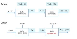
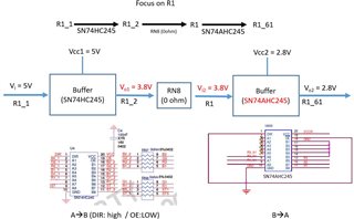
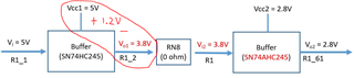
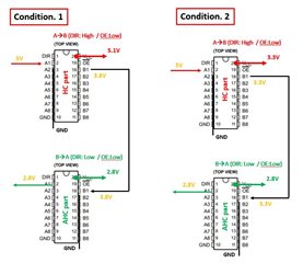
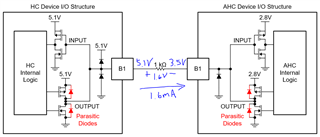
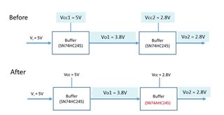
Below is my measurement. Could you let me know why Vo1 is clamped by Vcc2+1V? (when Vcc2 = 3.8V, Vo1 will be 4.8V)

Regards,

Roy

  • Hi Team,

    Excuse me. I would like to modify my measurement result showing as below. 

    We saw the second buffer input voltage will be Vcc2+1V. Will this let trace have large current? Why second input voltage will be clamped?

    Roy

  • HC family devices have ESD clamping diodes between the input pins and VCC; an uncontrolled current will flow into VCC2.
    AHC family devices do not have such diodes; their inputs are overvoltage tolerant, and no current will flow.

    See [FAQ] Can the input voltage (Vi) to my logic device be higher than the supply voltage (Vcc)?

    EDIT: On this device, all I/O pins also are outputs, so they do clamp.

  • Hi Ladisch,

    Both of HC and AHC have clamp issue. Even though, there is no current pass from Vin to Vcc, but there is voltage drop on the trace. We concerned that the voltage drop caused the high current.

    We would like to know why voltage clamp occurred in our application.  Could you solve it?

    Roy

  • No such voltage drop should happen with an AHC input alone.

    Please show the schematic of your circuit.

  • Hi Ladisch,

    Please see below. I have a mistake with previous image. The Vol and Vi2 = 3.8V. Is there any risk for front buffer?

    Roy

  • Nothing in the schematic explains this behavior.

    Is there anything else connected to R1_2 or R1?

    Can you double-check that U4 really is a HC device, and not some device with TTL outputs? Can you measure its input impedance (between VCC and R1_1)?

  • Hi Ladisch,

    1. There is no components between R1_2 or R1.

    2. we check the buffer is HC&AHC part.

    3. R1_1 to Vcc impedance is 4.3Mohm. 

    Roy

  • Hi Roy,

    Have you tried removing the devices/replacing them?

    From what you've described, it sounds like there's some issue with one of the devices - possibly damage to the output of the HC245 or to the input of the AHC245.

    Assuming that the output of the HC245 is driving HIGH, this 1.2V drop at the output of the SN74HC245 is much larger than it should be for a high-impedance input. Typically this type of drop would be caused by a large current draw at the output (~ 30mA). This could also be caused by a partial short to ground on the board.

  • Hi Maier,

    We think the 3.8V issue is from AHC part. (2.8V+1V) And so the HC part is the result. So we are not sure whether there is risk in HC part. (1.2V across you said) May you use EVM board to test our condition? Just cascade the HC part and AHC part. I think you may duplicate the issue.

    Roy

  • Have you tried removing the devices/replacing them?

  • Hi Maier,

    Yes, we had removed and replace the new HC and AHC part. We have five signal rail using HC + AHC parts and all of them have clamp issue. If we disconnect the AHC part, the HC part output is ok.(follow Vcc1)

    Roy

  • Can you insert a small resistor into the line (replace RN8, or at other places) to check whether a current flows at that point?

  • Hi Ladisch,

    I used the 14-24-LOGIC-EVM to do the measurement. The result is the same as my customer. And I showed the result without any signal input. Please show below config.

    In condition. 1, the 100ohm has 0.52 voltage drop and both of HC part and AHC part input voltage is ok.

    In condition. 2, as you see, I connect the HC part B1 rail to the AHC part B1 rail. And I find the AHC part Vcc will be 3.64V even if my power supply input voltage is 2.8V.(Power supply shows the 3.6V on the screen if I connect the trace. If I disconnect the trace, the AHC part input voltage will be 2.8V, like condition. 3.)


    Regards,

    Roy

  • Sorry; I just realized that this is a transceiver, where all I/O pins are both inputs and inputs. Therefore, all I/Os have clamping diodes.

    To get a device with overvoltage-tolerant inputs, you need a unidirectional buffer, e.g., SN74AHC244 or SN74AHC541.

  • Hi Ladisch,

    Excuse me. Let's back to original question and forget previous test result. Below is result by using customer application.

    Condition. 2 is ok to us, but condition. 1 is abnormal. We expect that we could see the 5V on HC part instead of 3.8V. It looks something clamp the voltage. 

    Do you think this is the normal situation? 

    Could you let me know the your idea? And does it have any risk for the result?

    Roy

  • All A/B pins of the AHC245 are outputs, so they indeed clamp the voltage (even when the outputs on that side are inactive).

  • Hi Ladisch,

    But inside AHC part, there is no positive clamp diode. Why the voltage will be clamped when we used HC+AHC part?

    Also why 3.3V is ok to our design? 

    Any risk in our result?

    Roy 

  • AHC does have positive clamp diodes on the outputs. The B1 pin can be an output, so it has clamp diodes.

    The difference between 3.3 V and 2.8 V is so small that only a small current flows.

  • Hi Ladisch,

    Sorry for typo. HC part doesn't have positive ESD diode. So in our application, we may need HC part combo to avoid clamp voltage issue, is it correct?

    And the voltage clamp is occurred by AHC part?

    Roy

  • Hi Roy,

    The HC family of logic also has clamp diodes and will not resolve this issue.

    Perhaps an illustration will be of some help.

    Each transceiver device has both input and output structures connected to the pin. When you try to drive the output of the HC device to 5.1V, this forward biases the output parasitic diode across the p-channel MOSFET in the AHC device, which causes the voltage to clamp to 2.8V + Vf, with Vf being the forward voltage of the diode (depends on current flow).

    The best solution here is to add a series resistor to limit current flow through the diode:

    You can use larger values of resistance to limit the current further if necessary -- this is primarily limited by the parasitic capacitance in the system and the speed required.

    You could also switch to using a voltage translation device such as SN74LVC8T245, which has dual supplies and enables communication between voltage nodes.