Other Parts Discussed in Thread: SYSCONFIG
Hello,
we tried updateing the SDK to 08.05 and postponed the new flash-driver in 08.04 already. So we wanted to finally update it but experiences problems as described in https://e2e.ti.com/support/microcontrollers/arm-based-microcontrollers-group/arm-based-microcontrollers/f/arm-based-microcontrollers-forum/1189521/mcu-plus-sdk-am243x-loadcpus-sometimes-asserts-in-dma-access/4521992#4521992
with the IS25WX256T it does not seem to work, at least the read data is not correct.
I will copy the observation from the other thread:
so I compared the init of both sdks. First I let the old one run, which works. I copied all the issued flash-cmds for config inside Flash_norOspiOpen and copied the register values to compare them. The only difference I see is the order of the address-byte setting. But the registers seem to be the same in the end. I let both run until
attackVectorStatus = OSPI_phyReadAttackVector(obj->ospiHandle, phyTuningOffset);
since this is the point where we get different results when reading the flash.
Every indendation means this is the value/call inside the function above.
for the old working drivers:
Flash_norOspiReadId
Flash_norOspiCmdRead(config, cmd(0x9F), cmdAddr(OSPI_CMD_INVALID_ADDR), numAddrBytes(0), idCode, numRdIdBytes(5))
OSPI_setDeviceSize(obj->ospiHandle, attrs->pageSize, attrs->blockSize)
OSPI0__OSPI_CFG_VBUSP__VBP2APB_WRAP__OSPI_CFG_VBP__OSPI_FLASH_APB_REGS_dev_size_config_reg 0x00111002 Device Size Configuration Register [Memory Mapped]
OSPI_setCmdExtType(obj->ospiHandle, OSPI_CMD_EXT_TYPE_INVERSE)
obj->cmdExtType = cmdExtType;
obj->dtrEnable = OSPI_isDtrEnable(obj->ospiHandle); (1)
OSPI_getXferLines(obj->ospiHandle) (3/OCTAL)
Flash_norOspiEnable4ByteAddr(config)
Flash_norOspiCmdWrite(config, devDefines->NOR_CMD_WREN(0x06), OSPI_CMD_INVALID_ADDR, 0, NULL, 0)
Flash_norOspiCmdWrite(config, devDefines->NOR_CMD_WRCR2(0x81), devDefines->NOR_ADDRESS_CONFIG_REG_ADDR(0x5), 3, ®Data(0xFE), 1);
Flash_norOspiCmdWrite(config, ((Flash_NorOspiDevDefines *)config->devDefines)->NOR_CMD_4BEN(0xB7), OSPI_CMD_INVALID_ADDR, 0, NULL, 0);
OSPI_setNumAddrBytes(obj->ospiHandle, 4)
OSPI0__OSPI_CFG_VBUSP__VBP2APB_WRAP__OSPI_CFG_VBP__OSPI_FLASH_APB_REGS_dev_size_config_reg 0x00111003 Device Size Configuration Register [Memory Mapped]
Flash_norOspiEnableDDR(config)
Flash_norOspiCmdWrite(config, devDefines->NOR_CMD_WREN(0x06), OSPI_CMD_INVALID_ADDR, 0, NULL, 0);
Flash_norOspiCmdWrite(config, devDefines->NOR_CMD_WRCR2(0x81), devDefines->NOR_DDR_EN_REG_ADDR(0), 4, ®Data(0xE7), 1);
OSPI_enableDDR(obj->ospiHandle)
OSPI0__OSPI_CFG_VBUSP__VBP2APB_WRAP__OSPI_CFG_VBP__OSPI_FLASH_APB_REGS_config_reg 0x81783801 Octal-SPI Configuration Register [Memory Mapped]
obj->xferLines = OSPI_XFER_LINES_OCTAL;
Flash_norOspiSetOpcodes(config)
readCmd = devDefines->NOR_CMD_OCTAL_READ_DDR;
progCmd = devDefines->NOR_CMD_PAGE_PROG;
OSPI_setXferLines(obj->ospiHandle, obj->xferLines);
OSPI0__OSPI_CFG_VBUSP__VBP2APB_WRAP__OSPI_CFG_VBP__OSPI_FLASH_APB_REGS_dev_instr_rd_config_reg 0x00033303 Device Read Instruction Configuration Register [Memory Mapped]
OSPI0__OSPI_CFG_VBUSP__VBP2APB_WRAP__OSPI_CFG_VBP__OSPI_FLASH_APB_REGS_dev_instr_wr_config_reg 0x00033002 Device Write Instruction Configuration Register [Memory Mapped]
obj->xferLines = xferLines;
OSPI_setXferOpCodes(obj->ospiHandle, readCmd, progCmd)
OSPI0__OSPI_CFG_VBUSP__VBP2APB_WRAP__OSPI_CFG_VBP__OSPI_FLASH_APB_REGS_dev_instr_rd_config_reg 0x000333FD Device Read Instruction Configuration Register [Memory Mapped]
OSPI0__OSPI_CFG_VBUSP__VBP2APB_WRAP__OSPI_CFG_VBP__OSPI_FLASH_APB_REGS_opcode_ext_lower_reg 0x02EDFA7A Opcode Extension Register (Lower) [Memory Mapped]
OSPI0__OSPI_CFG_VBUSP__VBP2APB_WRAP__OSPI_CFG_VBP__OSPI_FLASH_APB_REGS_dev_instr_wr_config_reg 0x00033012 Device Write Instruction Configuration Register [Memory Mapped]
OSPI0__OSPI_CFG_VBUSP__VBP2APB_WRAP__OSPI_CFG_VBP__OSPI_FLASH_APB_REGS_opcode_ext_lower_reg 0x02EDFA7A Opcode Extension Register (Lower) [Memory Mapped]
Flash_norOspiSetDummyCycles(config)
OSPI_setReadDummyCycles(obj->ospiHandle, rdDummyCycles)
OSPI0__OSPI_CFG_VBUSP__VBP2APB_WRAP__OSPI_CFG_VBP__OSPI_FLASH_APB_REGS_dev_instr_rd_config_reg 0x100333FD Device Read Instruction Configuration Register [Memory Mapped]
OSPI_setCmdDummyCycles(obj->ospiHandle, cmdDummyCycles)
OSPI0__OSPI_CFG_VBUSP__VBP2APB_WRAP__OSPI_CFG_VBP__OSPI_FLASH_APB_REGS_flash_cmd_ctrl_reg 0x810B8400 Flash Command Control Register [Memory Mapped]
OSPI_setDualOpCodeMode(obj->ospiHandle)
OSPI0__OSPI_CFG_VBUSP__VBP2APB_WRAP__OSPI_CFG_VBP__OSPI_FLASH_APB_REGS_config_reg 0xC1783801 Octal-SPI Configuration Register [Memory Mapped]
Flash_norOspiRegRead(config, devDefines->NOR_DUMMY_CYCLE_PROG_REG_ADDR(0x1), ®Data(0x1F)
Flash_norOspiRegWrite(config, devDefines->NOR_DUMMY_CYCLE_PROG_REG_ADDR, regData(0x10))
OSPI_setRdDataCaptureDelay(obj->ospiHandle, readDataCapDelay);
OSPI0__OSPI_CFG_VBUSP__VBP2APB_WRAP__OSPI_CFG_VBP__OSPI_FLASH_APB_REGS_rd_data_capture_reg 0x00000127 Read Data Capture Register [Memory Mapped]
OSPI0__OSPI_CFG_VBUSP__VBP2APB_WRAP__OSPI_CFG_VBP__OSPI_FLASH_APB_REGS_config_reg 0xC1783881 Octal-SPI Configuration Register [Memory Mapped]
for the new updated - not working - driver:
OSPI_setDeviceSize
OSPI0__OSPI_CFG_VBUSP__VBP2APB_WRAP__OSPI_CFG_VBP__OSPI_FLASH_APB_REGS_dev_size_config_reg 0x00111002 Device Size Configuration Register [Memory Mapped]
OSPI_setCmdExtType
obj->cmdExtType = cmdExtType;
obj->numAddrBytes = 3;
obj->currentProtocol = FLASH_CFG_PROTO_1S_1S_1S;
Flash_norOspiSetProtocol
Flash_set888mode
Flash_norOspiRegRead(config, octCfg->cmdRegRd (0x85), octCfg->cfgReg (0), ® (0xFF))
Flash_norOspiRegWrite(config, octCfg->cmdRegWr (0x81), octCfg->cfgReg (0), reg (0xE7));
OSPI_setProtocol((OSPI_Handle)(obj->ospiHandle), gFlashToSpiProtocolMap[pCfg->protocol]);
OSPI0__OSPI_CFG_VBUSP__VBP2APB_WRAP__OSPI_CFG_VBP__OSPI_FLASH_APB_REGS_dev_instr_rd_config_reg 0x00033303 Device Read Instruction Configuration Register [Memory Mapped]
OSPI0__OSPI_CFG_VBUSP__VBP2APB_WRAP__OSPI_CFG_VBP__OSPI_FLASH_APB_REGS_dev_instr_wr_config_reg 0x00033002 Device Write Instruction Configuration Register [Memory Mapped]
OSPI_enableDDR(handle)
OSPI0__OSPI_CFG_VBUSP__VBP2APB_WRAP__OSPI_CFG_VBP__OSPI_FLASH_APB_REGS_config_reg 0x81783801 Octal-SPI Configuration Register [Memory Mapped]
OSPI_setDualOpCodeMode(handle)
OSPI0__OSPI_CFG_VBUSP__VBP2APB_WRAP__OSPI_CFG_VBP__OSPI_FLASH_APB_REGS_config_reg 0xC1783801 Octal-SPI Configuration Register [Memory Mapped]
obj->protocol = protocol;
obj->currentProtocol = pCfg->protocol;
OSPI_setProtocol((OSPI_Handle)ospiHandle, gFlashToSpiProtocolMap[protocol]);
obj->currentProtocol = config->devConfig->protocolCfg.protocol;
Flash_norOspiSetAddressBytes(config, obj->ospiHandle)
Flash_norOspiSet4ByteAddrMode
Flash_norOspiCmdWrite(config, devCfg->cmdWren(0x06), OSPI_CMD_INVALID_ADDR, 0, NULL, 0);
Flash_norOspiCmdWrite(config, 0xB7, OSPI_CMD_INVALID_ADDR, 0, NULL, 0);
obj->numAddrBytes = 4;
OSPI_setNumAddrBytes(ospiHandle, 4);
OSPI0__OSPI_CFG_VBUSP__VBP2APB_WRAP__OSPI_CFG_VBP__OSPI_FLASH_APB_REGS_dev_size_config_reg 0x00111003 Device Size Configuration Register [Memory Mapped]
obj->numAddrBytes = numAddrBytes;
OSPI_setXferOpCodes(obj->ospiHandle, config->devConfig->protocolCfg.cmdRd, config->devConfig->protocolCfg.cmdWr);
OSPI0__OSPI_CFG_VBUSP__VBP2APB_WRAP__OSPI_CFG_VBP__OSPI_FLASH_APB_REGS_dev_instr_rd_config_reg 0x000333FD Device Read Instruction Configuration Register [Memory Mapped]
OSPI_getCmdExt
case OSPI_CMD_EXT_TYPE_INVERSE:
cmdExt = ~cmd;
OSPI0__OSPI_CFG_VBUSP__VBP2APB_WRAP__OSPI_CFG_VBP__OSPI_FLASH_APB_REGS_opcode_ext_lower_reg 0x0202FA7A Opcode Extension Register (Lower) [Memory Mapped]
OSPI0__OSPI_CFG_VBUSP__VBP2APB_WRAP__OSPI_CFG_VBP__OSPI_FLASH_APB_REGS_dev_instr_wr_config_reg 0x00033012 Device Write Instruction Configuration Register [Memory Mapped]
OSPI0__OSPI_CFG_VBUSP__VBP2APB_WRAP__OSPI_CFG_VBP__OSPI_FLASH_APB_REGS_opcode_ext_lower_reg 0x02EDFA7A Opcode Extension Register (Lower) [Memory Mapped]
Flash_norOspiSetModeDummy(config, obj->ospiHandle)
OSPI_setReadDummyCycles(ospiHandle, pCfg->dummyClksRd)
OSPI0__OSPI_CFG_VBUSP__VBP2APB_WRAP__OSPI_CFG_VBP__OSPI_FLASH_APB_REGS_dev_instr_rd_config_reg 0x100333FD Device Read Instruction Configuration Register [Memory Mapped]
obj->rdDummyCycles = dummyCycles;
OSPI_setCmdDummyCycles(ospiHandle, pCfg->dummyClksCmd)
OSPI0__OSPI_CFG_VBUSP__VBP2APB_WRAP__OSPI_CFG_VBP__OSPI_FLASH_APB_REGS_flash_cmd_ctrl_reg 0x810A8400 Flash Command Control Register [Memory Mapped]
obj->cmdDummyCycles = dummyCycles;
Flash_norOspiSetRegCfg(config, dCfg)
Flash_norOspiRegRead(config, rCfg->cmdRegRd(0x85), rCfg->cfgReg(0x1), &cfgReg(0x1F))
Flash_norOspiRegWrite(config, rCfg->cmdRegWr, rCfg->cfgReg, cfgReg(0x10))
OSPI_setRdDataCaptureDelay(obj->ospiHandle, readDataCapDelay)
OSPI0__OSPI_CFG_VBUSP__VBP2APB_WRAP__OSPI_CFG_VBP__OSPI_FLASH_APB_REGS_rd_data_capture_reg 0x00000127 Read Data Capture Register [Memory Mapped]
OSPI_phyReadAttackVector
OSPI0__OSPI_CFG_VBUSP__VBP2APB_WRAP__OSPI_CFG_VBP__OSPI_FLASH_APB_REGS_config_reg 0xC1783881 Octal-SPI Configuration Register [Memory Mapped]
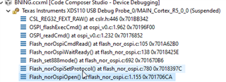
I also noticed that, when trying to do a CPU reset via ccs and load the image again after the call of the mentioned OSPI_phyReadAttackVector, the first read in SDR config won't work anymore and thus we can't read out the flash-id. We do - independently of the driver - have the same sequence you use in your driver-example:
    OSPI_norFlashSetCmds(0x03, 0x02, 0xD8);

    /* Initialize the flash device in 1s1s1s mode */
    OSPI_norFlashInit1s1s1s(ospiObject_.handle);
    /* Read ID */
    status = OSPI_norFlashReadId(ospiObject_.handle, &manfId, &deviceId);
This always worked with the old driver. With the new driver we need a power reset of the device to get this working. Else the read stuff is not correct. I guess the driver configures something different here but I don't know what.
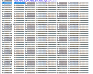
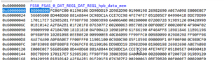
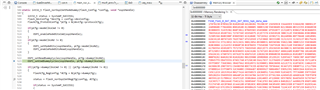
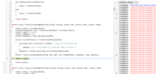
Also some screenshots of how the read out memory looks after the call of OSPI_phyReadAttackVector at 0x60000000 via memory browser:
old driver:


it seems only some values match and then somehow all memory after that has the same value. Maybe that helps to identify the problem better.
Additionally here is our new configuration that I migrated:
#define FLASH_SIZE (32U * 1024U * 1024U)
#define FLASH_BLOCK_SIZE (128U * 1024U)
#define FLASH_SECTOR_SIZE (4U * 1024U)
#define FLASH_PAGE_SIZE (256U)
#define FLASH_NUM_BLOCKS (FLASH_SIZE / FLASH_BLOCK_SIZE)
#define FLASH_NUM_PAGES_PER_BLOCK (FLASH_BLOCK_SIZE / FLASH_PAGE_SIZE)
#define FLASH_NUM_SECTORS (FLASH_SIZE / FLASH_SECTOR_SIZE)
Flash_DevConfig gFlashDevCfg_IS25WX256T =
{
.cmdExtType = OSPI_CMD_EXT_TYPE_INVERSE,
.enable4BAddr = TRUE,
.addrByteSupport = 1,
.fourByteAddrEnSeq = 0x02, // NOR_CMD_4BEN
.cmdWren = 0x06, // NOR_CMD_WREN
.cmdRdsr = 0x05, // NOR_CMD_RDSR
.srWip = (1 << 0), // NOR_SR_WIP
.srWel = (1 << 1),
.xspiWipRdCmd = 0x00,
.xspiWipReg = 0x00000000,
.xspiWipBit = (1 << 0),
.resetType = 0x10, // NOR_CMD_RSTEN/NOR_CMD_RST_MEM
.eraseCfg = {
.blockSize = FLASH_BLOCK_SIZE,
.sectorSize = FLASH_SECTOR_SIZE,
.cmdBlockErase3B = 0xD8, // NOR_CMD_BLOCK_ERASE
.cmdBlockErase4B = 0xDC, // NOR_CMD_BLOCK_ERASE
.cmdSectorErase3B = 0x20, // NOR_CMD_SECTOR_ERASE
.cmdSectorErase4B = 0x21, // NOR_CMD_SECTOR_ERASE
.cmdChipErase = 0xC7, // NOR_CMD_BULK_ERASE
},
.idCfg = {
.cmd = 0x9F, /* Constant */ // NOR_CMD_RDID
.numBytes = 5, // NOR_RDID_NUM_BYTES
.dummy4 = 0,
.dummy8 = 0,
},
.protocolCfg = {
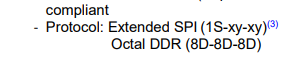
.protocol = FLASH_CFG_PROTO_8D_8D_8D,
.isDtr = TRUE,
.cmdRd = 0xFD, // NOR_CMD_OCTAL_READ_DDR
.cmdWr = 0x12, // NOR_CMD_PAGE_PROG
.modeClksCmd = 0,
.modeClksRd = 0,
.dummyClksCmd = 8, // NOR_OCTAL_CMD_READ_DUMMY_CYCLE
.dummyClksRd = 16, // NOR_OCTAL_READ_DUMMY_CYCLE
.enableType = 0,
.enableSeq = 0,
.protoCfg = {
.isAddrReg = TRUE,
.cmdRegRd = 0x85, // NOR_CMD_RDCR2
.cmdRegWr = 0x81, // NOR_CMD_WRCR2
.cfgReg = 0x00000000, // NOR_DDR_EN_REG_ADDR
.shift = 0,
.mask = 0xFF,
.cfgRegBitP = 0xE7, // NOR_DDR_EN_REG_DATA
},
.strDtrCfg = {
.isAddrReg = TRUE,
.cmdRegRd = 0x85, // NOR_CMD_RDCR2
.cmdRegWr = 0x81, // NOR_CMD_WRCR2
.cfgReg = 0x00000000, // NOR_DDR_EN_REG_ADDR
.shift = 0,
.mask = 0xFF,
.cfgRegBitP = 0xE7, // NOR_DDR_EN_REG_DATA
},
.dummyCfg = {
.isAddrReg = TRUE,
.cmdRegRd = 0x85, // NOR_CMD_RDCR2
.cmdRegWr = 0x81, // NOR_CMD_WRCR2
.cfgReg = 0x00000001, // NOR_DUMMY_CYCLE_PROG_REG_ADDR
.shift = 0,
.mask = 0xFF,
.cfgRegBitP = 16, // NOR_OCTAL_READ_DUMMY_CYCLE
},
},
.flashWriteTimeout = 120, // NOR_PAGE_PROG_TIMEOUT
.flashBusyTimeout = 256000000,
};
Flash_Attrs gFlashAttrs_IS25WX256 =
{
.flashName = "IS25WX256",
.deviceId = 0x5B19,
.manufacturerId = 0x9D,
.flashSize = FLASH_SIZE,
.blockCount = FLASH_NUM_BLOCKS,
.blockSize = FLASH_BLOCK_SIZE,
.pageCount = FLASH_NUM_PAGES_PER_BLOCK,
.pageSize = FLASH_PAGE_SIZE,
.sectorCount = FLASH_NUM_SECTORS,
.sectorSize = FLASH_SECTOR_SIZE,
};
is there maybe another point inside the sdk that was changed that could have an impact here? But all other drivers are working fine. mcspi, pruicss, icssemac, clock, hwtimer, adc, gpios and so on are working as expected.
Also pls mention: I removed the subsequent Flash_norOspiReadId of the new driver, which was used to calculate the readDataCapDelay, since this never worked (it counted down to 0). I just set it hard to 3 which was the value of the old driver. But also this did not work.
The setting of the old driver were:
#include <board/flash.h>

Flash_NorOspiDevDefines gFlashNorOspiDeviceDefines_IS25WX256 = {

    .NOR_CMD_RSTEN                       = 0x66U,
    .NOR_CMD_RST_MEM                     = 0x99U,
    .NOR_CMD_WREN                        = 0x06U,
    .NOR_CMD_WRDI                        = 0x04U,
    .NOR_CMD_RDCR                        = 0x00U,
    .NOR_CMD_WRCR                        = 0x01U,
    .NOR_CMD_RDCR2                       = 0x85U,
    .NOR_CMD_RDCR2_NVO                   = 0xB5U,
    .NOR_CMD_WRCR2                       = 0x81U,
    .NOR_CMD_WRCR2_NVO                   = 0xB1U,
    .NOR_CMD_BULK_ERASE                  = 0xC7U,
    .NOR_CMD_BLOCK_ERASE                 = 0xDCU,
    .NOR_CMD_SECTOR_ERASE                = 0x21U,
    .NOR_CMD_RDSR                        = 0x05U,
    .NOR_CMD_RDID                        = 0x9FU,
    .NOR_CMD_RDSFDP                      = 0x5AU,
    .NOR_CMD_READ                        = 0x03U,
    .NOR_CMD_OCTAL_READ_SDR              = 0xCCU,
    .NOR_CMD_OCTAL_READ_DDR              = 0xFDU,
    .NOR_CMD_PAGE_PROG                   = 0x12U,
    .NOR_CMD_4BEN                        = 0xB7U,
    .NOR_SR_WIP                          = (1U << 0U),
    .NOR_RDID_NUM_BYTES                  = 0x5U,
    .NOR_MANF_ID                         = 0x9DU,
    .NOR_DEVICE_ID                       = 0x5B19U,
    .NOR_SINGLE_CMD_READ_DUMMY_CYCLE     = 0U,
    .NOR_OCTAL_CMD_READ_DUMMY_CYCLE      = 8U,
    .NOR_OCTAL_READ_DUMMY_CYCLE          = 16U,
    .NOR_OCTAL_READ_LC                   = 16U,
    .NOR_OCTAL_READ_DATA_CAP_DELAY       = 3U,
    .NOR_DDR_EN_REG_DATA                 = 0xE7U,
    .NOR_DDR_EN_REG_ADDR                 = 0x00000000U,
    .NOR_DUMMY_CYCLE_PROG_REG_ADDR       = 0x00000001U,
    .NOR_ADDRESS_CONFIG_REG_ADDR         = 0x00000005U,
    .NOR_WRR_WRITE_TIMEOUT               = 1200U,
    .NOR_BULK_ERASE_TIMEOUT              = 72000000,
    .NOR_PAGE_PROG_TIMEOUT               = 120U,
    .NOR_PAGE_SIZE                       = 256U,
};

#define FLASH_SIZE                  (32U * 1024U * 1024U)
#define FLASH_BLOCK_SIZE            (128U * 1024U)
#define FLASH_SECTOR_SIZE           (4U * 1024U)
#define FLASH_PAGE_SIZE             (256U)
#define FLASH_NUM_BLOCKS            (FLASH_SIZE / FLASH_BLOCK_SIZE)
#define FLASH_NUM_PAGES_PER_BLOCK   (FLASH_BLOCK_SIZE / FLASH_PAGE_SIZE)
#define FLASH_NUM_SECTORS           (FLASH_SIZE / FLASH_SECTOR_SIZE)

Flash_Attrs gFlashNorOspiAttrs_IS25WX256 =
{
    .deviceId       = 0,  /* filled by Flash_open, after querying the flash */
    .manufacturerId = 0,  /* filled by Flash_open, after querying the flash */
    .driverInstance = 0,  /* filled by SysConfig */
    .flashSize      = FLASH_SIZE,
    .blockCount     = FLASH_NUM_BLOCKS,
    .blockSize      = FLASH_BLOCK_SIZE,
    .pageCount      = FLASH_NUM_PAGES_PER_BLOCK,
    .pageSize       = FLASH_PAGE_SIZE,
    .sectorSize     = FLASH_SECTOR_SIZE,
    .sectorCount    = FLASH_NUM_SECTORS,
};
We need the flash-driver to be working with the new sdk.
Best regards
Felix