This thread has been locked.

If you have a related question, please click the "Ask a related question" button in the top right corner. The newly created question will be automatically linked to this question.

TM4C123GH6PM: SSIDataGet blocking for SPI slave

Part Number: TM4C123GH6PM

Hi, I'm using a pair of TM4C123G evaluation boards trying to get an SSI channel to work. These boards have TM4C123GH6PM microcontrollers. I'm using a recent version of Code Composer Studio and TivaWare 2.2.0.295.

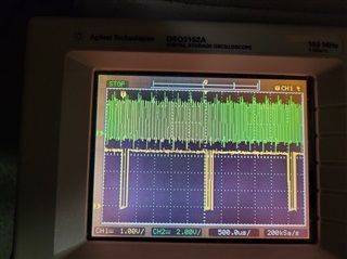
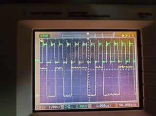
Between the boards we have SSI1 clock connected, and SSI1 RX/TX crosswired - RX on board 1 connects to TX on board 2 and vice versa. I have two CCS projects, a SPI master and a SPI slave. I'm simply trying to transmit "1234" from master to slave twice a second. We've looked at the lines on a scope, we see a 1 MHz clock and 2 Hz data. From that it seems the master side is working as expected. This issue I have is on the slave. After setup I'm in a loop trying to read data, and the first call to SSIDataGet never returns. Code for both sides below. What am I doing wrong ?!

// SPI master
#include <stdint.h>
#include "inc/hw_memmap.h"
#include "driverlib/gpio.h"
#include "driverlib/pin_map.h"
#include "driverlib/ssi.h"
#include "driverlib/sysctl.h"
#include "driverlib/uart.h"

/////////////////////////////////////////////////////////////////////////////
void InitializeSystem()
{
    // Set the clocking to run directly from the crystal.
    SysCtlClockSet(SYSCTL_SYSDIV_1 | SYSCTL_USE_OSC | SYSCTL_OSC_MAIN | SYSCTL_XTAL_16MHZ);

    // Initialize UART1 to 115200 baud, N-8-1
    // UART1 : GPIO Port B : UART1RX = PB0 : UART1TX = PB1
    SysCtlPeripheralEnable(SYSCTL_PERIPH_UART1);
    SysCtlPeripheralEnable(SYSCTL_PERIPH_GPIOB);

    GPIOPinConfigure(GPIO_PB0_U1RX);
    GPIOPinConfigure(GPIO_PB1_U1TX);

    GPIOPinTypeUART(GPIO_PORTB_BASE, GPIO_PIN_0 | GPIO_PIN_1);

    UARTConfigSetExpClk(UART1_BASE, SysCtlClockGet(), 115200,
                        UART_CONFIG_WLEN_8 | UART_CONFIG_STOP_ONE | UART_CONFIG_PAR_NONE);
}

/////////////////////////////////////////////////////////////////////////////
void InitializeSSI1()
{
    // Enable the SSI1 peripheral for use.
    SysCtlPeripheralEnable(SYSCTL_PERIPH_SSI1);

    // We have PD0 (SSI1 Clk), PD2 (SSI1 Rx), and PD3 (SSI1 Tx) connected.
    // (Odd thing, pins/ports for SSI1 are the same as SSI3 ?!)
    SysCtlPeripheralEnable(SYSCTL_PERIPH_GPIOD);

    // Configure the pin muxing for SSI functions
    GPIOPinConfigure(GPIO_PD0_SSI1CLK);
    GPIOPinConfigure(GPIO_PD1_SSI1FSS);
    GPIOPinConfigure(GPIO_PD2_SSI1RX);
    GPIOPinConfigure(GPIO_PD3_SSI1TX);

    // Configure the GPIO settings for the SSI pins.  This function also gives
    // control of these pins to the SSI hardware.
    GPIOPinTypeSSI(GPIO_PORTD_BASE, GPIO_PIN_0 | GPIO_PIN_1 | GPIO_PIN_2 | GPIO_PIN_3);

    // Configure and enable the SSI port for SPI master mode.
    SSIDisable(SSI1_BASE);
    SSIConfigSetExpClk(SSI1_BASE, SysCtlClockGet(), SSI_FRF_MOTO_MODE_0, SSI_MODE_MASTER, 1000000, 8);

    // Advance mode settings. Legacy is default. I've seen several mentions
    // in technical forum discussions that when writing as SSI master, you
    // need "dummy" reads (in legacy mode)?
    //SSIAdvModeSet(SSI1_BASE, SSI_ADV_MODE_WRITE);

    // Enable the SSI module.
    SSIEnable(SSI1_BASE);

    // Read residual data from the SSI port so we don't read any junk.
    uint32_t RxData;
    while (SSIDataGetNonBlocking(SSI1_BASE, &RxData))
    {
    }
}

/////////////////////////////////////////////////////////////////////////////
int main(void)
{
    InitializeSystem();
    InitializeSSI1();

    // A call to SysCtlDelay with a delay count of 1 takes 3 clock cycles
    unsigned int nDelayOneMillisecond = (SysCtlClockGet() / 3) / 1000;
    const unsigned int nDelayCount = 500 /* milliseconds */ * nDelayOneMillisecond;

    const unsigned int Message[4] = { '1', '2', '3', '4' };
    uint32_t RxData = 0;
    while (true)
    {
        // Transmit on SPI and UART every <n> milliseconds.
        SysCtlDelay(nDelayCount);

        for (unsigned int nByte = 0 ; nByte < 4 ; nByte++)
        {
            while (SSIDataGetNonBlocking(SSI1_BASE, &RxData)) {}
            SSIDataPut(SSI1_BASE, Message[nByte]);
//            SSIDataGetNonBlocking(SSI1_BASE, &RxData);
            UARTCharPut(UART1_BASE, (unsigned char)Message[nByte]);
        }
    }
}

// SPI slave
#include <stdint.h>
#include "inc/hw_memmap.h"
#include "driverlib/gpio.h"
#include "driverlib/pin_map.h"
#include "driverlib/ssi.h"
#include "driverlib/sysctl.h"
#include "driverlib/uart.h"

/////////////////////////////////////////////////////////////////////////////
void InitializeSystem()
{
    // Set the clocking to run directly from the crystal.
    SysCtlClockSet(SYSCTL_SYSDIV_1 | SYSCTL_USE_OSC | SYSCTL_OSC_MAIN | SYSCTL_XTAL_16MHZ);

    // Initialize UART1 to 115200 baud, N-8-1
    // UART1 : GPIO Port B : UART1RX = PB0 : UART1TX = PB1
    SysCtlPeripheralEnable(SYSCTL_PERIPH_UART1);
    SysCtlPeripheralEnable(SYSCTL_PERIPH_GPIOB);

    GPIOPinConfigure(GPIO_PB0_U1RX);
    GPIOPinConfigure(GPIO_PB1_U1TX);

    GPIOPinTypeUART(GPIO_PORTB_BASE, GPIO_PIN_0 | GPIO_PIN_1);

    UARTConfigSetExpClk(UART1_BASE, SysCtlClockGet(), 115200,
                        UART_CONFIG_WLEN_8 | UART_CONFIG_STOP_ONE | UART_CONFIG_PAR_NONE);
}

/////////////////////////////////////////////////////////////////////////////
void InitializeSSI1()
{
    // Enable the SSI1 peripheral for use.
    SysCtlPeripheralEnable(SYSCTL_PERIPH_SSI1);

    // We have PD0 (SSI1 Clk), PD2 (SSI1 Rx), and PD3 (SSI1 Tx) connected.
    // (Odd thing, pins/ports for SSI1 are the same as SSI3 ?!)
    SysCtlPeripheralEnable(SYSCTL_PERIPH_GPIOD);

    // Configure the pin muxing for SSI functions
    GPIOPinConfigure(GPIO_PD0_SSI1CLK);
    GPIOPinConfigure(GPIO_PD1_SSI1FSS);
    GPIOPinConfigure(GPIO_PD2_SSI1RX);
    GPIOPinConfigure(GPIO_PD3_SSI1TX);

    // Configure the GPIO settings for the SSI pins.  This function also gives
    // control of these pins to the SSI hardware.
    GPIOPinTypeSSI(GPIO_PORTD_BASE, GPIO_PIN_0 | GPIO_PIN_1 | GPIO_PIN_2 | GPIO_PIN_3);

    // Configure and enable the SSI port for SPI slave mode.
    SSIDisable(SSI1_BASE);
    SSIConfigSetExpClk(SSI1_BASE, SysCtlClockGet(), SSI_FRF_MOTO_MODE_0, SSI_MODE_SLAVE, 1000000, 8);
    //SSIConfigSetExpClk(SSI1_BASE, SysCtlClockGet(), SSI_FRF_MOTO_MODE_0, SSI_MODE_SLAVE_OD, 1000000, 8);

    // Advance mode settings. Legacy is default.
    //SSIAdvModeSet(SSI1_BASE, SSI_ADV_MODE_LEGACY);

    // Enable the SSI module.
    SSIEnable(SSI1_BASE);

    // Read residual data from the SSI port so we don't read any junk.
    uint32_t RxData;
    while (SSIDataGetNonBlocking(SSI1_BASE, &RxData))
    {
    }
}

/////////////////////////////////////////////////////////////////////////////
int main(void)
{
    // Initialize the system
    InitializeSystem();
    InitializeSSI1();

    unsigned int nByte = 0;
    while (true)
    {
        // Get next charater on SPI and forward to UART
        SSIDataPut(SSI1_BASE, 0); // dummy write?
        SSIDataGet(SSI1_BASE, &nByte);
        UARTCharPut(UART1_BASE, (unsigned char)nByte);
    }
}

  • We got this to work by connecting the FSS pins between the two boards. But we still have an issue, this needs to work without FSS. We're interfacing to inertial units using SDLC / SPI. We currently use MSP430s for this, they work fine, but we want to upgrade to the TM4Cs. The interface there only has clock and RX to the microcontrollers. Do all the MOTO modes require FSS? Is there a mode that doesn't? 

  • Hi David,

     TM4C123 as a master does not need the chip select to function. You could repurpose the Fss pin for GPIO pin if you want. It is the slave who needs the chip select for qualification.  For MOTO mode to work on TM4C123 as a slave device, you must have a chip select. However, that chip select does not need to be Fss as in your current setup using two different TM4C boards You can generate your own chip select by using a GPIO pin on the master side. The slave needs the chip select to qualify the sampling of data when the clock arrives. If you have a different slave device that does not need the chip select then it will sample data upon receiving the clock from the master. However, I have not come across a slave device that does not need the chip select.

  • Thank you Charles, I think this helps. Please don't lock the thread yet.

    The person who did the MSP430 implementation is gone. Slave select is not connected there. The pin for that is multi-function and one of the other functions is selected. What we're guessing, based on your answer, is slave select when not selected is in a state that tells the slave that data is always valid. The software matches that, it's reading continually, including all filler between actual data. ?!

  • Hi David,

      When you write back to this thread, the thread will automatically set the status to open and I will be notified. 

  • I dug deeper into the existing MSP430 design that is working. That has an STE (slave transmit enable) for SPI in addition to clock and data. So STE is the same as Fss on the TM4C? The MSP430 has a 3-pin mode in which STE is not used, and that is the mode we're using.

    Per your response FSS is required for a SPI slave on the TM4C. So there is no equivalent to the 3-pin mode on the MSP430?

    On the pair of TM4C evaluation boards, running SPI master on one and SPI slave on the other, it worked in MOTO_MODE_3 with the FSS just grounded on the slave, not connected to the boards. But tried that on SPI slave connected to the sensor we're trying to listen to and the data is still not right. We have the sensor output split to go to both an MSP430 and a TM4C, the MSP430 still reads the data correctly.

  • Hi,

    But tried that on SPI slave connected to the sensor we're trying to listen to and the data is still not right.

    Can you elaborate what is not right? 

    Per your response FSS is required for a SPI slave on the TM4C. So there is no equivalent to the 3-pin mode on the MSP430?

    Reading the datasheet again, it has the below description about mode 0 and mode 2. You will need Fss for these two modes. 

    However, in the case of continuous back-to-back transmissions, the SSInFss signal must be pulsed
    High between each data word transfer because the slave select pin freezes the data in its serial
    peripheral register and does not allow it to be altered if the SPH bit is clear. Therefore, the master
    device must raise the SSInFss pin of the slave device between each data transfer to enable the
    serial peripheral data write. On completion of the continuous transfer, the SSInFss pin is returned
    to its idle state one SSInClk period after the last bit has been captured.

    On the pair of TM4C evaluation boards, running SPI master on one and SPI slave on the other, it worked in MOTO_MODE_3 with the FSS just grounded on the slave, not connected to the boards

    For mode 1 and mode 3, below is the description. 

    uous back-to-back transmissions, the SSInFss pin remains in its active Low state until
    the final bit of the last word has been captured and then returns to its idle state as described above.


    For continuous back-to-back transfers, the SSInFss pin is held Low between successive data words
    and termination is the same as that of the single word transfer.

  • Can you elaborate what is not right? 

    A couple of things. The incoming data uses SDLC, there is supposed to be a sync at start and end of actual data composed of six 1 bits preceded and followed by a zero bit. The message between those is about 30 bytes. In between messages and sync markers are filled with xFF. I took the MSP430 code over to the TM4C as closely as possible. It finds start and end sync on the MSP430, it only works occasionally on the TM4C. Most of the time on the TM4C it doesn't find sync, some of the time it does but early, other times it's close.

    We also modified the hardware we're working with so that sensor clock and RX output goes to both an MSP430 and a TM4C. I put software on both to simply take SPI input and transmit out a UART after discarding the xFF filler. And recorded both at the same time on a PC. It's different. I can find a unique byte sequence in the MSP430 output, and can't find same in TM4C output. And vice versa

    Both of the above are in MOTO_MODE_3 with FSS grounded.  From the description of mode 1 & 3 it sounds like that should work? But there's noise coming in from something.

  • Small update. We checked the UCA control registers in the MSP430. They're set to clock polarity 0, clock phase 1, 8-bit, 3-pin SPI slave. So we retested on the TM4C using MOTO_MODE_1, incoming data is still not clean.

  • Hi,

      It is true that between bytes the Fss (chip select) is held low. However, I wonder with Fss tied to GND, the slave state machine does not know when is the correct beginning of a transfer.  

    If the QSSI is enabled and valid data is in the transmit FIFO, the start of transmission is signified
    by the SSInFss master signal being driven Low. The master SSInDAT0/SSInTX output is enabled.
    After an additional one-half SSInClk period, both master and slave valid data are enabled onto
    their respective transmission lines. At the same time, the SSInClk is enabled with a rising edge
    transition.

    It finds start and end sync on the MSP430, it only works occasionally on the TM4C. Most of the time on the TM4C it doesn't find sync, some of the time it does but early, other times it's close.

    Do you see any error in SSI such as Receive Timeout ?

    The message between those is about 30 bytes. In between messages and sync markers are filled with xFF.

    What is the duration between bytes within a message? How long is the gap between message? Since the Fss is tied to ground, please make sure time-out  counter is reset o

    The RX FIFO has an associated time-out counter which starts to down count at the same time the
    RX FIFO is flagged as not empty by the RNE bit in the SSISR register. The counter is reset any time 

    a new or next byte is written to the RX FIFO, thus the counter will continue to count down to zero
    unless there is new activity. The time-out period is 32 periods based on the period of SSInClk.
    When the counter reaches zero, a time-out interrupt bit, RTRIS, is set in the SSIRIS register. The
    time-out interrupt can be cleared by writing a 1 to the RTIC bit of the SSI Interrupt Clear (SSIIC)
    register or by emptying the RX FIFO. If the interrupt is cleared and there is residual data left in the
    RX FIFO or new data entries have been written, the timer count down initiates and the interrupt will
    be reasserted after 32 periods have been counted.

    Before you start the slave, did you first clear the receive FIFO?

    //
    // Read any residual data from the SSI port. This makes sure the receive
    // FIFOs are empty, so we don't read any unwanted junk. This is done here
    // because the SPI SSI mode is full-duplex, which allows you to send and
    // receive at the same time. The SSIDataGetNonBlocking function returns
    // "true" when data was returned, and "false" when no data was returned.
    // The "non-blocking" function checks if there is any data in the receive
    // FIFO and does not "hang" if there isn't.
    //
    while(SSIDataGetNonBlocking(SSI0_BASE, &pui32DataRx[0]))
    {
    }

  • I tried to upload images of the clock & data lines from a scope, they look like they upload but then nothing shows up in the preview pane.

    The messages come out at ~400 Hz. Clock line from then sensor (SPI master) is1.0152 MHz, and is always running. On the scope you can see each message is ~0.25 milliseconds long, then the data line is high for 2.25 milliseconds until the next message. And you can see that rising edge of the clock is centered on each data bit.

    I don't see receive timeouts. I'm using the blocking SSI call to read data. I added the following preceding the reads :

                nInterruptStatus = SSIIntStatus(SSI1_BASE, false);
                if ((nInterruptStatus & SSI_RXTO) != 0)
                {
                    nTimeoutCount++;
                }
                SSIDataGet(SSI1_BASE, &nData);
    

    I let that run for awhile in the debugger then break and timeout count is zero. And I'd expect that, because the clock is always there, and the data line is high between messages, the reads between messages are returning 0xFF, and there is always something to read.

    Yes I do clear the receive FIFO before starting the slave, that is at the bottom of InitializeSSI1 in the code samples I originally uploaded. I am doing that after enabling SSI1, that's how it was done in all the samples I've seen.

  • Hi,

      You can drag the file into the editor. If you still have problem then capture the images into a file and then drag the file over. It is good to see the images but with your description I should be clear about the questions I asked. 

      I have some questions:

      - Does the slave fail to capture the first message correctly or it is always some later messages?

      - If you focus just on the the first message, does the slave correctly decode the start (01111110b) and end (01111110b) of the message?

      - I think the answers to above questions will help answer if the problem is due to the absence of Fss - where the slave is unable to recognize the first bit of a SPI transfer.

      - I will suggest you send out the received data on the TX pin instead of sending out dummy '0'. This way you can view both RX and TX on a logic analyzer. This is easier to see where TX and RX starts to deviate. 

  • I see the images but this is just what is sent by the master. I can't really decipher it. Can you please answer the questions I asked earlier. Logic analyzer will greatly facilitate debugging especially for stream of messages. 

  • I modified the code to write out to SPI Tx each byte right after it was received by SSIDataGet. Also have switched back to MOTO_MODE_3, that matches TM4C documentation best, slave select low and data bits sampled on rising clock edge.

    Focusing on the first message. Messages are 31 to 33 bytes in length. I did 10 runs in the debugger, with a breakpoint set where the code either thinks it has seen both start and end markers for a message, or knows it has gone too far (> 60 bytes) without finding the end marker. Just went to the first breakpoint, the first message. Only one of the runs looked like it might be legitimate, the rest were either stopped after 60 bytes or early.

    I'm also running the same code on the MSP430, on the same input. It finds both start and end markers every time, with end always coming 31 to 33 bytes after start.

    We do not have a logic analyzer. If you think that's critical we'll find a way. I really appreciate your help.

  • Hi David,

    Focusing on the first message. Messages are 31 to 33 bytes in length. I did 10 runs in the debugger, with a breakpoint set where the code either thinks it has seen both start and end markers for a message, or knows it has gone too far (> 60 bytes) without finding the end marker. Just went to the first breakpoint, the first message. Only one of the runs looked like it might be legitimate, the rest were either stopped after 60 bytes or early.

    First of all, I really think a logic analyzer is worth the investment especially for debugging your current problem, it will come really handy. Logic analyzer these days can decode most of the communication protocols you can think of, not just SPI. So you can use it for debugging other protocols as well. You can capture up to a second of traces depending on the model. That is a lot of data to capture. I'm not endorsing any particular model. You can do some search that is best for your development. 

    Only one of the runs looked like it might be legitimate, the rest were either stopped after 60 bytes or early.

    I have yet to know if the issue is related to software or hardware. Therefore, we need some experiments.

      - Can you focus just on the Start Marker which is 01111110b. Can your external master only sends the Start Marker? Can you always reliably receive this 01111110b? This is only one byte. If you can't even receive this byte then I don't think it is a software issue. If you can't control the master from generating further bytes then at least configure your scope to trigger on the first edge of the clock. How does the TX and RX look?

      - To isolate if it is a hardware issue, I will suggest you control the Fss input pin to the slave using another GPIO pin. First assert the Fss pin high before the slave is initialize and right before you are about to start the master transmission, assert the Fss low. Can you reliably capture the start marker and the first message? If the presence of Fss (signifying the start of SPI trasnfer) makes a difference then we kind of know the problem is related to the Fss pin. If the receive still craps out somewhere, maybe it has something to do with the software. 

     - How are using processing the received data? Are you using interrupt? Are you using UARTprintf() to send the data to the terminal? I'd like to know how you are doing your software. The reason I ask is that UART is running much slower than SPI. If you are waiting for UART to complete the transmit, there may be more data being received by the SPI. In another word, UART may not keep up with SPI. If you are using UART in blocking mode, you may lose data in SSI RXFIFO. From what I know so far, it is not losing data but rather capturing wrong data, is that correct?

  • I think there's a break in the case. I wrote test applications to do what you suggested, simply look for the start marker. I did the MSP430 first, it worked fine. Then I did the TM4C, with identical scanning code from the MSP430. It didn't work. But ... then I check endianess of the bit stream. On the TM4C the bits are inverted, MSB is what LSB is on the MSP430. I switched the TM4C to invert scanning per that, and it's successfully finding start markers now. I checked the MSB/LSB last week, but must have made a mistake. Now I'm going to look for the trailing sync to see if that works.

  • Hi David,

      That is a great find. Looks like you have narrowed the discrepancy between Tiva and MSP430. Let us know if you are able to scan the trailing sync successfully. 

  • I'm now reliably getting trailing sync as well. Thank you so much for your help!

    Here's a summary for anyone that ends up here.

    We are doing a hardware upgrade, and plan to use TM4Cs to replace MSP430s. We're interfacing with an IMU that uses SDLC and is a SPI master. We are only connected to SPI lines for clock and RX (TX from the IMU). There are two other lines involved, TX and FSS. We leave TX unconnected, that works on both the MSP430 and TM4C. The clock out of the IMU is always on.

    The MSP430 data sheet refers to the 4th SPI line as STE, not FSS, And we're using a 3-pin mode that ignores it. So on the MSP430 that is unconnected. It works fine, with the oddity that there is always data to read. Between actual data frames the lines are tri-stated, which reads as 0xFFs.

    To get similar code to work on the TM4C, we didn't find a 3-pin mode. What seems to be working is running in SSI_FRF_MOTO_MODE_3 with FSS grounded. For MOTO_MODE_3, FSS is low when data is valid. Grounding it appears to tell SPI slave in Mode 3 that data is always valid. With that we get 0xFF filler between data as we do on the MSP430. And the final piece of the puzzle was the bit stream was inverted on the TM4C from what it was on the MSP430. Taking that into account we are now finding the SDLC start and end markers bracketing data in the bit stream. Also for what it's worth we're using SSI_MODE_SLAVE_OD since we only listen :

    SSIConfigSetExpClk(SSI1_BASE, SysCtlClockGet(), SSI_FRF_MOTO_MODE_3, SSI_MODE_SLAVE_OD, 1000000, 8);