This thread has been locked.
If you have a related question, please click the "Ask a related question" button in the top right corner. The newly created question will be automatically linked to this question.
Hi,
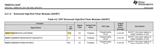
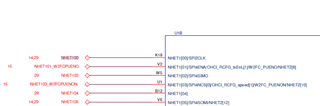
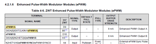
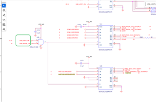
I am trying to use TMDX570LC43HDK to drive a motor, but in the user guide(link below) cant see any PWM signal out. So my first question is from which pin we can get the signal. I have also check the TMDX570LC43HDK Schematics, but same no PWM.
https://www.ti.com/lit/ug/spnu597a/spnu597a.pdf?ts=1708932415689
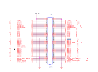
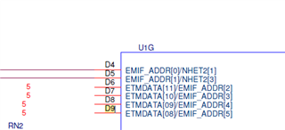
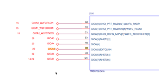
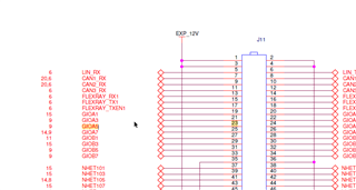
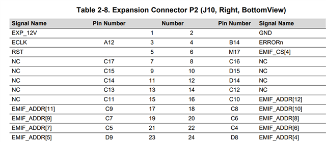
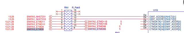
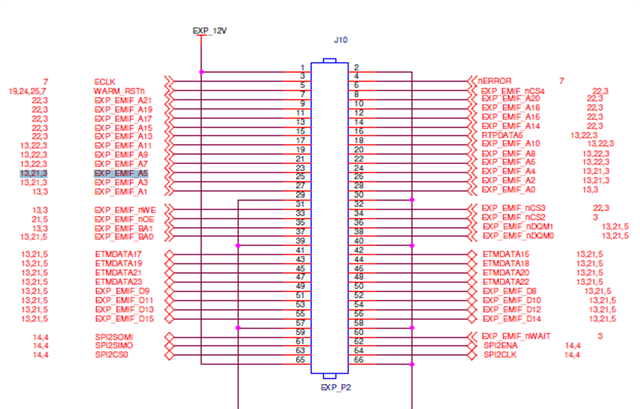
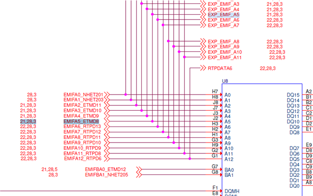
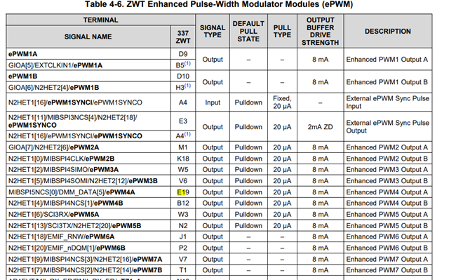
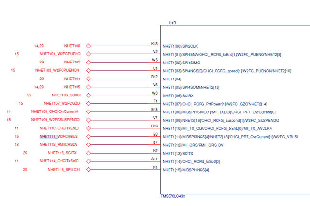
My next question is TMDX570LC43HDK connector (for example: J9,J10,J11) how it aligns with TMS570LC435 processor pin out. For example: D9 exist in both table , but the signal name doesn't match.
Thanks
Hi Mohammad,
I started working on this thread now and will provide you an update ASAP.
—
Thanks & regards,
Jagadish.
Hi Mohammad,
It depends on the module you are using to generate the PWM:
The PWM in this device can be generated from different peripherals like ePWM, NHET and eCAP etc. can be used for to generate the PWM.
Example-2:
Hercules Tutorial: Using the NHET to generate a PWM (youtube.com)
If you refer above tutorial then there NHET was used to generate the PWM, And in above example the PWM was generated on the NHET1[0] pin which is nothing but K18 pin of the controller:
And if you verify this pin in the schematic of HDK, this was connected to the
pin 38 of J11 connector.
Example-2:
In above example i used ePWM module to generate the PWM and i generated the PWM on ePWM1A pin
According to datasheet ePWM1A can be generate on D9 and/or B5 pins of the controller:
As you can see D9 pin have only one functionality that is ePWM1A, so that means ePWM1A waveform will always generate on this pin. However you can also generate the ePWM1A waveform on B5 pin as well by configuring corresponding functionality as below:
If we do this then our PWM waveform will generate on the both the pins D9 and B5 as below:
I created this example on the Launchpad, so i verified where B5 and D9 pins are connected in the lauchpad:
D9 was connected to the 17th pin of J10 connector.
B5 was connected to the 7th pin of J4 connector and i verified the waveforms from the respective pins.
If you are using HDK then:
D9 is not routed to anywhere from the controller:
B5 was connected to the 23rd pin of J11 connector
--
Thanks & regards,
Jagadish.
Hi Jagadish,
Thank you for your reply, K19 looks ok to me now, but if we see D9 on HDK User guide(www.ti.com/.../spnu597a.pdf D9 is connected on J10 pin 23
on the other hand the schematics ( https://www.ti.com/lit/zip/spnr043) D9 looks open here and not terminating on J10 on this schematics.
If we further trace back in schematics J10 pin 23 is connected U8 J2.
Then from U8 its connected to U1C microcontroller E9. I am bit confused how J10 pin 23 is connected to E9, as in HDK user guide its saying connected with D9
Then from UC1 E9 connected to the RN1.
So in conclusion it looks schematic and HDK manual guide doesn't match, can you please advice from which connector pin D9 signal be can found and how HDK user guide and Schematics interlinked and also can you double check that both document align each other in all aspect.
Hi Mohammad,
We are sorry for these typos. And thanks for pointing out this again. We will correct this one in our next document release.
In HDK schematic D9 was not connected to any pin.
--
Thanks & regards,
Jagadish.
Hi Jagadish
I am not sure which document is correct SPNU597A ( https://www.ti.com/lit/ug/spnu597a/spnu597a.pdf?ts=1708932415689) or Schematics (https://www.ti.com/lit/zip/spnr043), can you please pint out and also if possible can give a idea when the next document could be release.
Thanks
Mohammed Afzal
Hi Mohammed,
Please follow schematic, it was correct only except above typo.
can you please pint out and also if possible can give a idea when the next document could be release.
There is no plan yet and i have to discuss with my internal team on this.
--
Thanks & regards,
Jagadish.
Hi Jagadish,
I am not clear using some of the HDK pins, My first question is can we use GIO pin to generate PWM signal in HDK (https://www.ti.com/lit/zip/spnr043). For example if we take M1 pin from HDK schematics, which is saying its GIO,
But according to the micro data sheet (www.ti.com/.../tms570lc4357.pdf, it can be used as GIOA[7]/N2HET2[6]/ePWM2A. So my question is can we use M1 in HDK as ePWM.
And my second some of the pin like V7 connected to a Mux in HDK schematics, can we use this pin to generate PWM, according to the micro data sheet (TMS570LC4357) V7 can be used to create PWM.
Thanks
Mohammed Afzal
Hi Mohammed Afzal,
But according to the micro data sheet (www.ti.com/.../tms570lc4357.pdf, it can be used as GIOA[7]/N2HET2[6]/ePWM2A. So my question is can we use M1 in HDK as ePWM.
Yes M1 pin can be configured as ePWM pin.
For this purpose you just need to enable corresponding functionality in HALCoGen Pin mux table.
And my second some of the pin like V7 connected to a Mux in HDK schematics, can we use this pin to generate PWM, according to the micro data sheet (TMS570LC4357) V7 can be used to create PWM.
Yes it is connected to the mux.
Using the selection lines to the mux, we can operate this pin either USB functioanlity or the other functionalities like N2HET or ePWM.
To operate this pin as ePWM, just you should need to OFF the USB_HOST1_ON and USB_DEVICE_ON.
--
Thanks & regards,
Jagadish.