Other Parts Discussed in Thread: ADS1605
Related to locked thread:
Please forgive the "newbie" questions here, but I'm temporarily filling in for the real processor hardware and software people, and I'm not a processor guy. 
I need to connect two 16-bit parallel ADCs (ADS1605 : https://www.ti.com/lit/ds/symlink/ads1605.pdf ) to an ADS2434 R5 (AM2434BSDFHIALVR, the 441-pin ALV FCBGA) and read them at a 1.25 MSPS (800 ns) rate without using the PRU.
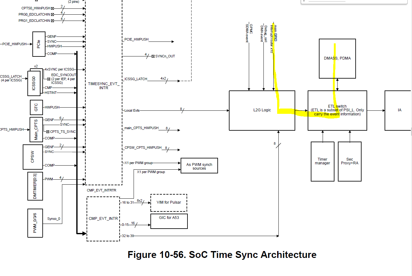
This seems to leave GPIO as a good option, since we have lots of spare GPIO pins, and couldn't find delta-sigma ADCs with adequate sample rate / bandwidth and true SPI outputs compatible with the 2434's native MCSPI ports. There is a high-priority goal to not have an FPGA or other external logic in the interface -- we need it to be glue-free between the ADCs and the CPU.
The biggest question is whether the 2434 can do these parallel ADC reads "automatically" via hardware peripherals and write the samples into a buffer via DMA without bogging down the processor.
The two ADS1605 ADCs will run from the same external low-jitter sample oscillator and be synchronized via the reset pin to provide coherent/simultaneous sampling.
The DRDY pin will go low when each new sample is ready (every 800 ns), and since the two ADCs are synchronized, only one DRDY signal is needed as a GPIO (interrupt?) input to tell the processor to go grab the data.
GPIOs on the 2434 appear to be grouped into banks of 16 bits each. Since I need to read two 16-bit ADCs, it would be OK if this is done as one 32-bit read, with the words separated later in software, but if it can be done as two 16-bit reads, that is also OK.
As an added nuance, I would also like to read the overrange (OTR) pin from each ADC simultaneously with the data, but that makes each input a 17-bit read (34 bits total per sample). I could replace the LSB from each ADC with the OTR bit and treat the input data as a 15-bit ADC, but that is not ideal.
If the inputs can be read in groups of 32 bits and it's possible to DMA two streams on each DRDY pulse, then I could read ADC data as a 17-bit word (16 data + 1 OTR, ignore other 15) from each ADC.
If the inputs have to be read in groups of 16 bits, then it would be three reads per DRDY pulse: 16 bits from first ADC, then 16 bits from second ADC, then two OTR bits with 14 bits ignored on the third read.
Presumably the ADC CS and RD pins could be asserted (low) all the time, and no bit-banging would be required other than whatever it takes for the CPU to read those 34 data pins before the next DRDY falling edge.
However the data streaming works out, I can't go interrupting the processor every 800 ns to read converters. I need between 4096 and 4608 samples from each ADC to get stored in a buffer by DMA before the processor is interrupted or scheduled to go process the frame.
It would be ideal to alternate the storage between ping and pong buffers.
It would be acceptable to "interrupt" the processor on either a "buffer full" status (reached programmable end limit between 4096 and 4608) or on a timer interrupt (period = buffer size * sample rate).
With me not being a processor guy and the 2434 TRM being over 10K pages... I'm struggling to commit a board layout for this architecture without some confirmation the parallel interface will work in this scenario. It seems this was all much easier when using SPI or MCBSP...
Any input you can provide on the pin/bank assignments (for data/OTR status) and pin assignment (GPIO, clock, other?) for the DRDY pulse, as well as peripheral configuration (DMA, Timer, Interrupt, GPIO) and software architecture in general would be really, really appreciated.
Many thanks!