AM2431: MCSPI Transfer Format

Part Number: AM2431
Other Parts Discussed in Thread: SYSCONFIG

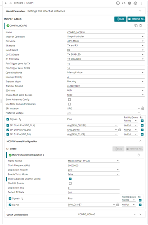
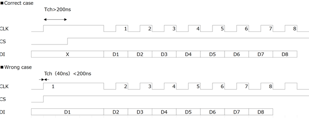
I am using MCSPI with MODE 3.

1.How can the results of setting POL and PHA for MCSPI_CHCONF_0/1/2/3[1],[2] be reflected in the output?

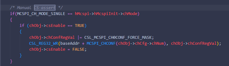
Currently, just setting POL=1 and PHA=1 does not make SPI_CLK high.
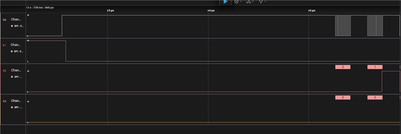
After that, SPI communication is performed (MCSPI_CHCONF register FORCE=1), SPI_CLK goes high and operation starts.
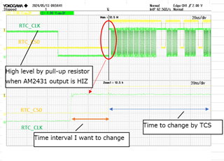
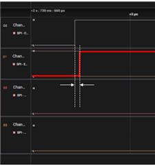
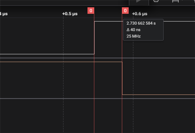
At this time, the time between the rising edge of SPI_CLK and the assertion edge of SPI_CS is too short to meet the hold time of the external SPI device.

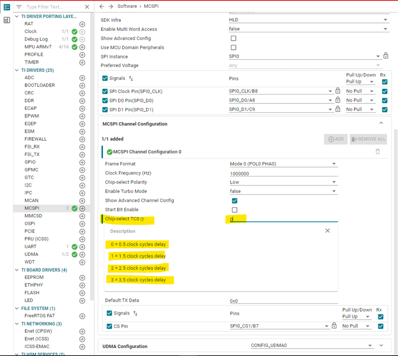
2. How can the time between the rising edge of SPI_CLK and the assertion edge of SPI_CS be increased?

  • Hi Futoshi,

    So the SPI settings all depends mutually on the Controller and the Peripheral.

    So the Controller which in this case is AM243 SoC supports all CPOL and CPHA combinations, namely 0, 1, 2 and 3 modes.

    But, the peripheral might not. So, I would request you to look through the Peripheral's datasheet and check which mode they support.

    You would also need to verify if the frequency your SPI clock is operating at is supported by the Peripheral's operating clock frequency.

    Apart from this, you need to make sure your code SPI Transaction Parameters are correctly initialized for a specific chip select line, lets say default CS0.

    Can you please tell me the specific SPI peripheral number you are using? And please also check the above mentioned parameters I asked to verify.

    Regards,

    Vaibhav

  • Hi Vaibhav

    I am not a good English speaker, so I may not be communicating well, but I would like to get an answer to my question.
    I am not talking about the peripherals working/not working.
    The peripheral is MODE3.
    After turning on the AM2431 and executing initialization processes such as PAD_CONFIG, I set POL=1 and PHA=1 on MCSPI_CHCONF_0/1/2/3[1],[2].
    At the time of just setting POL=1 and PHA=1 to MCSPI_CHCONF_0/1/2/3[1],[2], the inactive level of the SPI clock is at the LOW level.

    Q1. After setting POL=1 and PHA=1 to MCSPI_CHCONF_0/1/2/3[1],[2], which register should be set to change the inactive level of SPI clock on AM2431 output to HIGH level?

    When I set FORCE=1 in the MCSPI_CHCONF register to start SPI communication, the inactive level of SPI clock changes to HIGH level.

    The time from the rising edge of the SPI clock inactivity level changing to the HIGH level until CS is asserted is short.

    Q2: How can I increase the time between the SPI clock inactivity level changing to HIGH level and CS being asserted?

  • Hi Futoshi,

    Please expect responses in sometime.

    Regards,

    Vaibhav

  • Hi Vaibhav

    Noted.

    We look forward to your response.

    Best regards

  • Hi Vaibhav

    How are things progressing?

    Best regards

  • Greetings Futoshi,

    Thank you for your patience.

    Before moving forward, I would highly encourage you to look at MCSPI Loopback example which comes along with the MCU PLUS SDK. It can be found under MCU_PLUS_SDK_INSTALL_PATH>examples>drivers>mcspi

    Please also go through: https://software-dl.ti.com/mcu-plus-sdk/esd/AM243X/09_02_00_50/exports/docs/api_guide_am243x/EXAMPLES_DRIVERS_MCSPI_LOOPBACK.html

    Regards,

    Vaibhav

  • Hi Futoshi,

    To address your two queries.

    Q1. After setting POL=1 and PHA=1 to MCSPI_CHCONF_0/1/2/3[1],[2], which register should be set to change the inactive level of SPI clock on AM2431 output to HIGH level?

    So, currently for SW flow, you just need to assert the CS line and that will take care of the SPI Clock's output level from going low to high.

    I am also going to point out the relevant code section for the same.

    For interrupt mode, look at the API:  MCSPI_transferControllerIntr()

    For polled mode, look at the API:  MCSPI_transferControllerPoll()

    Here is a snippet of the code where CS gets asserted manually:

    Q2: How can I increase the time between the SPI clock inactivity level changing to HIGH level and CS being asserted?

    This time can be increased by setting a field in the SysConfig tool.

    Please find the attached image.

    Hope this answers your doubts. 

    Regards,

    Vaibhav

  • Hi Vaibhav,

    Even if I set Chip Select TCS, the time from when the SPI clock inactivity level changes to HIGH until CS is asserted does not change.

    The datasheet states, "This 2-bit field defines the number of interface clock cycles between CS toggling and the first or last edge of the MCSPI clock."

    This is different from what I want to change.

    How can I increase the time between the SPI clock inactivity level changing to HIGH level and CS being asserted?

  • Hello Futoshi,

    I am checking via logic analyzer by modifying some values from SysConfig.

    I am going to ask few follow up questions if needed.

    Please expect responses in sometime.

    Regards,

    Vaibhav

  • Hello Futoshi,

    I have few follow up questions.

    I understand that you want to change the time between the MCSPI Clock(going from low to high state) and Chip Select being asserted.

    But, on my logic analyzer, the SW flow is as follows, and does not match your diagram.

    I have attached two diagrams. (Note: D0 is clock and D1 is chip select, D2 is data)

    At first the CS line is being asserted and then the clock goes high from inactive level.

    Same follows for the following attached image as well.

    Have you marked incorrectly in your diagram the clock and CS ?

    Looking forward to your response.

    Regards,

    Vaibhav

  • Hi Vaibhav,

    Sorry for the delay in getting back to you.

    The CLK and CS of the waveform I acquired are correct.

    When you acquired the waveform, was it set to MODE3?

    The CS in your waveform has the logic reversed.

    Are the CS logic settings correct?

    Regards,

  • Hi Futoshi,

    The operation into consideration was MODE0 itself and not MODE3.

    And the diagram I have attached is correct itself. If you look in the second row the chip select is first asserted/that is pulled down and then the cock(in first row) is initiated along with the data being read in the third row.

    This is how the operation should happen. 

    Please let me know if you got any more doubts on my explanation.

    Regards,

    Vaibhav

  • Hi Vaibhav,

    As I first posted, my question is about when to set MODE3.

    Regards,

  • Hello Futoshi,

    Then I will be setting my operation as well into MODE3 and get the probing going.

    Once I collect the waveform, then I can comment on the same.

    Best Regards,

    Vaibhav

  • Hi Vaibhav,

    How are things progressing?

    Best regards,

  • Hello Futoshi,

    Thank you very much for your patience.

    I am actively working on this.

    Please expect to hear back from me in few hours.

    Regards,

    Vaibhav

  • Hello Futoshi,

    This is my current settings for the logic analyzer Software.

    Here is the SysConfig setting.

    With the above settings when I run the example this what I get at the beginning of the transaction.

    First one is clock, second one is chip select.

    I see that the clock goes from low to high and then the chip select goes from high to low(deasserted).

    Is the above combination what you were referring to earlier ?

    Regards,

    Vaibhav

  • Hi Vaibhav,

    The logic of CHIP SELECT is inverted.

    It goes HIGH when asserted.

    In my environment, this time is short, about 40ns.

    What is the difference? Can you figure out the cause?

    Best regards,

  • Hello Futoshi,

    Thank you very much for your patience.

    I just checked on my setup.

    In my environment as well I see that the difference is 40 ns.

    So safe to say, this has been replicated on my setup.

    My follow up question would be:

    Do you need an explanation on why this time gap exists? Like you expected this to be 0 ns?

    Or you just need a way to have a value of x ns where x < 40 ns and x != 0?

    Looking forward to your response.

    Regards,

    Vaibhav

  • Hi Vaibhav,

    The hold time specification on the peripheral side is 200ns or longer.

    40ns does not satisfy this time and may result in wrong operation.

    Therefore, I would like to increase this time.

    Regards,

  • Hello Futoshi,

    I suppose that the hold time needs to be looked further into.

    I am going to check with the development team on this and get back to you.

    Regards,

    Vaibhav

  • Hi Vaibhav,

    How are things progressing?

    If it’s not possible to change the time between when the clock goes high and when CS is asserted, please let me know.

    We will consider alternative measures on our end.

    Best regards,

  • Hello Futoshi, 

    I am running few experiments at my end and checking the logic analyzer, so you can expect updates from my end in few hours.

    Regards,

    Vaibhav

  • Hello,

    So with the change in few fields as mentioned:

    and

    if you do not see the value increased to 200 ns then it is not possible, this coming from SW Dev team.

    Regards,

    Vaibhav

  • Hi Vaibhav,

    Thank you for your response.

    However, the issue was not resolved even after changing those registers.

    I understand that the time between when the clock goes high and when CS is asserted cannot be changed.

    I was able to increase the time using the following method before performing SPI communication:

    1. Set Bit1 (PIN34) of the MCSPI_MODULCTRL (address: 0x20100128) register to 1 to disable SPIEN.

    2. Set Bit20 (FORCE), Bit1 (POL), and Bit0 (PHA) of the MCSPI_CHCONF_0 (address: 0x2010012C) register to 1 to configure it to mode 3.

    3. Set Bit20 (FORCE) of the MCSPI_CHCONF_0 (address: 0x2010012C) register to 0.

    4. Set Bit1 (PIN34) of the MCSPI_MODULCTRL (address: 0x20100128) register to 0 to re-enable SPIEN mode.

    Thank you

  • Hello Futoshi,

    I was able to increase the time using the following method before performing SPI communication:

    1. Set Bit1 (PIN34) of the MCSPI_MODULCTRL (address: 0x20100128) register to 1 to disable SPIEN.

    2. Set Bit20 (FORCE), Bit1 (POL), and Bit0 (PHA) of the MCSPI_CHCONF_0 (address: 0x2010012C) register to 1 to configure it to mode 3.

    3. Set Bit20 (FORCE) of the MCSPI_CHCONF_0 (address: 0x2010012C) register to 0.

    4. Set Bit1 (PIN34) of the MCSPI_MODULCTRL (address: 0x20100128) register to 0 to re-enable SPIEN mode.

    Thank you for providing the detailed stpes.

    I am going to mark this thread closed if this is resolved now.

    Regards,

    Vaibhav