This thread has been locked.
If you have a related question, please click the "Ask a related question" button in the top right corner. The newly created question will be automatically linked to this question.
Tool/software:
Hello TI expert,
I have a question about the diagnostic measures for CBA9 - Error codes for invalid transactions. The security manual explains that this diagnostic measure is executed by hardware and generates a bus error. Then:
1. Can this diagnostic measure be received through the R5FSS0_CORE0_INTR_IN_133 interrupt? If so, does it require enabling other registers (such as err_intr_enable_set)? Does an interrupt need to be cleared in the interrupt callback?
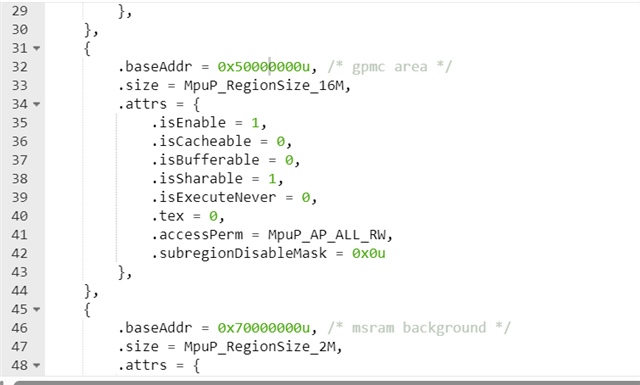
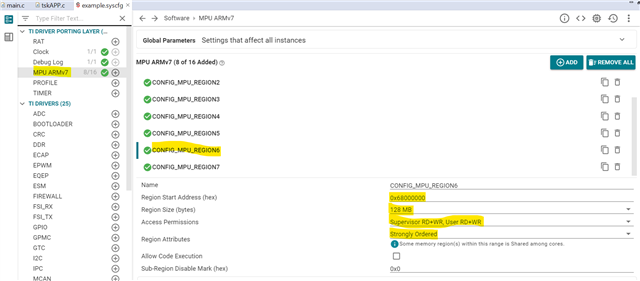
2. I need to test this diagnostic measure. Can I directly write data to the PCIE device address (0x69000000) for testing (in my project, PCIE devices are not used and have not been initialized). However, in my tests, after attempting to write, a data abort exception occurred.
Test log:
data abort:backtrace:
please use: addr2line -e rtthread.elf -a -f ffffffff828e9a60[17103] W/BACKTRACE: unwind: Unknown symbol address ffffffff828e9a60
[17103] W/BACKTRACE: unwind: Index not found ffffffff828e9a60
Execption:
r00:0x00000000 r01:0x69000000 r02:0xffffffff828e9a40 r03:0xffffffffffffffff
r04:0xffffffffdeadbeef r05:0xffffffffdeadbeef r06:0xffffffffdeadbeef r07:0xffffffffdeadbeef
r08:0xffffffffdeadbeef r09:0xffffffffdeadbeef r10:0xffffffffdeadbeef
fp :0xffffffffdeadbeef ip :0x00000000
sp :0xffffffff84001948 lr :0x700b1798 pc :0xffffffff828e9a68
cpsr:0x20000013
uint32_t ulTestData = 0U; void* hTransBufAddr = (void*)(CONFIG_PCIE0_OB_REG_L_TEST); memcpy(hTransBufAddr, &ulTestData, sizeof(uint32_t));
If there are issues with my approach, please give me some guidance. I need to test this diagnostic measure through event injection.
Thanks,
Best regards.
kaijie
Hello kaijie,
Sorry for the delayed reply as I was on leave yesterday.
You may get a reply in one or two days.
Regards,
Anil.
Hello kaijie,
1. Can this diagnostic measure be received through the R5FSS0_CORE0_INTR_IN_133 interrupt? If so, does it require enabling other registers (such as err_intr_enable_set)? Does an interrupt need to be cleared in the interrupt callback?
I am not sure if the CBA9 error will be generate to R5FSS0_CORE0_INTR_IN_133 interrupt or not.
I can move this thread to the right expert to comment on your issue.
But, typically, in R5F core, if a user wants to route an interrupt to R5F core, then users need to enable the interrupt otherwise, the interrupt will not be routed to R5f core.
Usually, enabling R5F interrupts we do follow below steps.
Coming to clear the interrupt, there is a master ISR in that already MCU+SDK will clear this interrupt. So, user no need to do it again.
Regards,
Anil.
HwiP_Params hwiPrms; HwiP_Object cmpHwiObject; /* Register pin interrupt */ HwiP_Params_init(&hwiPrms); hwiPrms.intNum = ; hwiPrms.priority = //4U; hwiPrms.callback = //&IsrFxn; hwiPrms.isPulse = //TRUE; retVal = HwiP_construct(&cmpHwiObject, &hwiPrms); DebugP_assert(retVal == SystemP_SUCCESS );
Anil:
Thank you for your response. Could you please direct me to another expert? Thank you.
kaijie
Hi kaijie,
Which SDK you are working?
Can you share details, step by step to reproduce the issue on our side?
Regards
Ashwani
Hi Ashwani,
The SDK package I am using is mcu_plus_sdk_am243x_09_00_00_35.
Implementation Process:
Prerequisites:
1. MPU has been enabled, and the address 0x69000000UL has read-write permissions.
2. DPL has been initialized.
3. There are no PCIE devices in the project, and none have been initialized.
Step One: By calling the DPL interface, I registered and enabled R5FSS0_CORE0_INTR_IN_133, (SDLR_R5FSS0_CORE0_INTR_GLUELOGIC_CBASS_INTR_OR_GLUE_MAIN_CBASS_AGG_ERR_INTR_0).
Step Two: An attempt was made to write data to the PCIE device at address 0x69000000UL.
Upon execution of the write, the system entered a data abort interrupt, after which it continuously executes the callback function registered for the R5FSS0_CORE0_INTR_IN_133 interrupt.
If there's an issue with my testing method, please guide me on how to conduct this diagnostic measure.
Thank you.
kaijie
Thanks kaijie,
Upon execution of the write, the system entered a data abort interrupt, after which it continuously executes the callback function registered for the R5FSS0_CORE0_INTR_IN_133 interrupt.
Is this not as per your expectation?
Implementation Process:
Prerequisites:
1. MPU has been enabled, and the address 0x69000000UL has read-write permissions.
2. DPL has been initialized.
3. There are no PCIE devices in the project, and none have been initialized.
Step One: By calling the DPL interface, I registered and enabled R5FSS0_CORE0_INTR_IN_133, (SDLR_R5FSS0_CORE0_INTR_GLUELOGIC_CBASS_INTR_OR_GLUE_MAIN_CBASS_AGG_ERR_INTR_0).
Step Two: An attempt was made to write data to the PCIE device at address 0x69000000UL.
What is your expectation with the test you mentioned above?
Regards
Ashwani
Hi Ashwani.
Thank you for your response.
Regarding your question, I expect that after executing the CBA9 diagnostic procedure test, only the registered R5FSS0_CORE0_INTR_IN_133 interrupt callback function will be called to record relevant information, without entering a data abort exception. In other words, the CPU needs to continue functioning normally.
Reference:
As stated in Section TRM3.4:"When CBASS detects an illegal transaction, it terminates the transaction gracefully to avoid a system hang. In addition, the CBASS sends return status back to the initiator with error status. If this illegal transaction is a read transaction, the read data is returned with all zeros. If this illegal transaction is a write transaction, this write transaction is terminated and returns a write error back to initiator. The interrupt and illegal transaction logging can be found in the CBASS’s err_regs region"
Therefore, I believe that after executing the test, only an error report will be generated without affecting the normal operation of the CPU. If my understanding is incorrect, please advise on how to perform the correct test for CBA9.
Best regards
kaijie
Thanks kaijie,
MPU has been enabled, and the address 0x69000000UL has read-write permissions
Can you share the snapshot of sysconfig and code base what you did for this region ?
Regards
Ashwani
I cannot upload screenshots, but I can provide code snippets. In our project, we haven't used the sysconfig tool for configuration. Here's the code for MPU setup:
MpuP_RegionConfig gMpuRegionConfig[CONFIG_MPU_NUM_REGIONS + 4] = { { .baseAddr = 0x0u, /* back groud */ .size = MpuP_RegionSize_4G, .attrs = { .isEnable = 1, .isCacheable = 0, .isBufferable = 0, .isSharable = 1, .isExecuteNever = 0, .tex = 0, .accessPerm = MpuP_AP_S_RW, .subregionDisableMask = 0x0u }, }, { .baseAddr = 0x0u, /* vectors */ .size = MpuP_RegionSize_32K, .attrs = { .isEnable = 1, .isCacheable = 1, .isBufferable = 1, .isSharable = 0, .isExecuteNever = 0, .tex = 1, .accessPerm = MpuP_AP_S_R, .subregionDisableMask = 0x0u }, }, { .baseAddr = 0x50000000u, /* gpmc area */ .size = MpuP_RegionSize_16M, .attrs = { .isEnable = 1, .isCacheable = 0, .isBufferable = 0, .isSharable = 1, .isExecuteNever = 0, .tex = 0, .accessPerm = MpuP_AP_ALL_RW, .subregionDisableMask = 0x0u }, }, { .baseAddr = 0x70000000u, /* msram background */ .size = MpuP_RegionSize_2M, .attrs = { .isEnable = 1, .isCacheable = 1, .isBufferable = 1, .isSharable = 0, .isExecuteNever = 0, .tex = 1, .accessPerm = MpuP_AP_ALL_RW, .subregionDisableMask = 0x0u }, }, { .baseAddr = 0x80000000u, /* ddr background */ .size = MpuP_RegionSize_2G, .attrs = { .isEnable = 1, .isCacheable = 1, .isBufferable = 1, .isSharable = 0, .isExecuteNever = 0, .tex = 1, .accessPerm = MpuP_AP_ALL_RW, .subregionDisableMask = 0x0u }, }, { .baseAddr = 0x70080000u, /* kernel code */ .size = MpuP_RegionSize_512K, .attrs = { .isEnable = 1, .isCacheable = 1, .isBufferable = 1, .isSharable = 0, .isExecuteNever = 0, .tex = 1, .accessPerm = MpuP_AP_S_RW, .subregionDisableMask = 0x0u }, }, { .baseAddr = 0x70100000u, /* kernel data */ .size = MpuP_RegionSize_512K, .attrs = { .isEnable = 1, .isCacheable = 1, .isBufferable = 1, .isSharable = 0, .isExecuteNever = 0, .tex = 1, .accessPerm = MpuP_AP_S_RW, .subregionDisableMask = 0x0u }, }, { .baseAddr = 0x84000000u, /* memheap */ .size = MpuP_RegionSize_128M, .attrs = { .isEnable = 1, .isCacheable = 1, .isBufferable = 1, .isSharable = 0, .isExecuteNever = 0, .tex = 1, .accessPerm = MpuP_AP_ALL_RW, .subregionDisableMask = 0x0u }, }, { .baseAddr = 0x80000000u, /* rodata */ .size = MpuP_RegionSize_8M, .attrs = { .isEnable = 1, .isCacheable = 1, .isBufferable = 1, .isSharable = 0, .isExecuteNever = 0, .tex = 1, .accessPerm = MpuP_AP_ALL_R, .subregionDisableMask = 0x0u }, }, { .baseAddr = 0x80800000u, /* kernel bss */ .size = MpuP_RegionSize_8M, .attrs = { .isEnable = 1, .isCacheable = 1, .isBufferable = 1, .isSharable = 0, .isExecuteNever = 0, .tex = 1, .accessPerm = MpuP_AP_S_RW, .subregionDisableMask = 0x0u }, }, };
Additionally, I tested it with elevated privileges.
Thanks and best regards.
kaijie
Hi Kaijie,
from your sysconfig, it seems that memory address 0x69000000UL is not enabled.
Below is what I have in my setup:
Let me know If I am missing something.
Regards
Ashwani
Hi Ashwani:
Thank you for your guidance. I do have an initialization issue here, but after modifying the MPU initialization, I attempted to write data to the address 0x69000000; however, I still encountered a data termination error.
Here are the revised MPU configurations I've tried:
MpuP_RegionConfig gMpuRegionConfig[CONFIG_MPU_NUM_REGIONS + 4] = { { .baseAddr = 0x0u, /* back groud */ .size = MpuP_RegionSize_4G, .attrs = { .isEnable = 1, .isCacheable = 0, .isBufferable = 0, .isSharable = 1, .isExecuteNever = 0, .tex = 0, .accessPerm = MpuP_AP_S_RW, .subregionDisableMask = 0x0u }, }, { .baseAddr = 0x0u, /* vectors */ .size = MpuP_RegionSize_32K, .attrs = { .isEnable = 1, .isCacheable = 1, .isBufferable = 1, .isSharable = 0, .isExecuteNever = 0, .tex = 1, .accessPerm = MpuP_AP_S_R, .subregionDisableMask = 0x0u }, }, { .baseAddr = 0x50000000u, /* gpmc area */ .size = MpuP_RegionSize_16M, .attrs = { .isEnable = 1, .isCacheable = 0, .isBufferable = 0, .isSharable = 1, .isExecuteNever = 0, .tex = 0, .accessPerm = MpuP_AP_ALL_RW, .subregionDisableMask = 0x0u }, }, { .baseAddr = 0x68000000u, /* PCIE */ .size = MpuP_RegionSize_128M, .attrs = { .isEnable = 1, .isCacheable = 1, .isBufferable = 1, .isSharable = 1, .isExecuteNever = 0, .tex = 0, .accessPerm = MpuP_AP_ALL_RW, .subregionDisableMask = 0x0u }, }, { .baseAddr = 0x70000000u, /* msram background */ .size = MpuP_RegionSize_2M, .attrs = { .isEnable = 1, .isCacheable = 1, .isBufferable = 1, .isSharable = 0, .isExecuteNever = 0, .tex = 1, .accessPerm = MpuP_AP_ALL_RW, .subregionDisableMask = 0x0u }, }, { .baseAddr = 0x80000000u, /* ddr background */ .size = MpuP_RegionSize_2G, .attrs = { .isEnable = 1, .isCacheable = 1, .isBufferable = 1, .isSharable = 0, .isExecuteNever = 0, .tex = 1, .accessPerm = MpuP_AP_ALL_RW, .subregionDisableMask = 0x0u }, }, { .baseAddr = 0x70080000u, /* kernel code */ .size = MpuP_RegionSize_512K, .attrs = { .isEnable = 1, .isCacheable = 1, .isBufferable = 1, .isSharable = 0, .isExecuteNever = 0, .tex = 1, .accessPerm = MpuP_AP_S_RW, .subregionDisableMask = 0x0u }, }, { .baseAddr = 0x70100000u, /* kernel data */ .size = MpuP_RegionSize_512K, .attrs = { .isEnable = 1, .isCacheable = 1, .isBufferable = 1, .isSharable = 0, .isExecuteNever = 0, .tex = 1, .accessPerm = MpuP_AP_S_RW, .subregionDisableMask = 0x0u }, }, { .baseAddr = 0x84000000u, /* memheap */ .size = MpuP_RegionSize_128M, .attrs = { .isEnable = 1, .isCacheable = 1, .isBufferable = 1, .isSharable = 0, .isExecuteNever = 0, .tex = 1, .accessPerm = MpuP_AP_ALL_RW, .subregionDisableMask = 0x0u }, }, { .baseAddr = 0x80000000u, /* rodata */ .size = MpuP_RegionSize_8M, .attrs = { .isEnable = 1, .isCacheable = 1, .isBufferable = 1, .isSharable = 0, .isExecuteNever = 0, .tex = 1, .accessPerm = MpuP_AP_ALL_R, .subregionDisableMask = 0x0u }, }, { .baseAddr = 0x80800000u, /* kernel bss */ .size = MpuP_RegionSize_8M, .attrs = { .isEnable = 1, .isCacheable = 1, .isBufferable = 1, .isSharable = 0, .isExecuteNever = 0, .tex = 1, .accessPerm = MpuP_AP_S_RW, .subregionDisableMask = 0x0u }, }, };
MpuP_RegionConfig gMpuRegionConfig[CONFIG_MPU_NUM_REGIONS + 4] = { { .baseAddr = 0x0u, /* back groud */ .size = MpuP_RegionSize_4G, .attrs = { .isEnable = 1, .isCacheable = 0, .isBufferable = 0, .isSharable = 1, .isExecuteNever = 0, .tex = 0, .accessPerm = MpuP_AP_S_RW, .subregionDisableMask = 0x0u }, }, { .baseAddr = 0x0u, /* vectors */ .size = MpuP_RegionSize_32K, .attrs = { .isEnable = 1, .isCacheable = 1, .isBufferable = 1, .isSharable = 0, .isExecuteNever = 0, .tex = 1, .accessPerm = MpuP_AP_S_R, .subregionDisableMask = 0x0u }, }, { .baseAddr = 0x50000000u, /* gpmc area */ .size = MpuP_RegionSize_16M, .attrs = { .isEnable = 1, .isCacheable = 0, .isBufferable = 0, .isSharable = 1, .isExecuteNever = 0, .tex = 0, .accessPerm = MpuP_AP_ALL_RW, .subregionDisableMask = 0x0u }, }, { .baseAddr = 0x68000000u, /* PCIE */ .size = MpuP_RegionSize_128M, .attrs = { .isEnable = 1, .isCacheable = 0, .isBufferable = 0, .isSharable = 1, .isExecuteNever = 0, .tex = 0, .accessPerm = MpuP_AP_ALL_RW, .subregionDisableMask = 0x0u }, }, { .baseAddr = 0x70000000u, /* msram background */ .size = MpuP_RegionSize_2M, .attrs = { .isEnable = 1, .isCacheable = 1, .isBufferable = 1, .isSharable = 0, .isExecuteNever = 0, .tex = 1, .accessPerm = MpuP_AP_ALL_RW, .subregionDisableMask = 0x0u }, }, { .baseAddr = 0x80000000u, /* ddr background */ .size = MpuP_RegionSize_2G, .attrs = { .isEnable = 1, .isCacheable = 1, .isBufferable = 1, .isSharable = 0, .isExecuteNever = 0, .tex = 1, .accessPerm = MpuP_AP_ALL_RW, .subregionDisableMask = 0x0u }, }, { .baseAddr = 0x70080000u, /* kernel code */ .size = MpuP_RegionSize_512K, .attrs = { .isEnable = 1, .isCacheable = 1, .isBufferable = 1, .isSharable = 0, .isExecuteNever = 0, .tex = 1, .accessPerm = MpuP_AP_S_RW, .subregionDisableMask = 0x0u }, }, { .baseAddr = 0x70100000u, /* kernel data */ .size = MpuP_RegionSize_512K, .attrs = { .isEnable = 1, .isCacheable = 1, .isBufferable = 1, .isSharable = 0, .isExecuteNever = 0, .tex = 1, .accessPerm = MpuP_AP_S_RW, .subregionDisableMask = 0x0u }, }, { .baseAddr = 0x84000000u, /* memheap */ .size = MpuP_RegionSize_128M, .attrs = { .isEnable = 1, .isCacheable = 1, .isBufferable = 1, .isSharable = 0, .isExecuteNever = 0, .tex = 1, .accessPerm = MpuP_AP_ALL_RW, .subregionDisableMask = 0x0u }, }, { .baseAddr = 0x80000000u, /* rodata */ .size = MpuP_RegionSize_8M, .attrs = { .isEnable = 1, .isCacheable = 1, .isBufferable = 1, .isSharable = 0, .isExecuteNever = 0, .tex = 1, .accessPerm = MpuP_AP_ALL_R, .subregionDisableMask = 0x0u }, }, { .baseAddr = 0x80800000u, /* kernel bss */ .size = MpuP_RegionSize_8M, .attrs = { .isEnable = 1, .isCacheable = 1, .isBufferable = 1, .isSharable = 0, .isExecuteNever = 0, .tex = 1, .accessPerm = MpuP_AP_S_RW, .subregionDisableMask = 0x0u }, }, };
kaijie
Hello, Expert.
Do you have any updates on this issue?
Thank you
Best regards
kaijie
HI Kaijie,
When you wite PCIE data area, could you please check the devlice power state is on ? I checked the TRM page 2622 of Rev.H. and found the LPSC_PCIe_0 default state is OFF, if you haven't enalbe this node , when you access this area, the CBA BUS ERROR will happen.
Thanks.
Linjun