This thread has been locked.
If you have a related question, please click the "Ask a related question" button in the top right corner. The newly created question will be automatically linked to this question.
Hello Support,
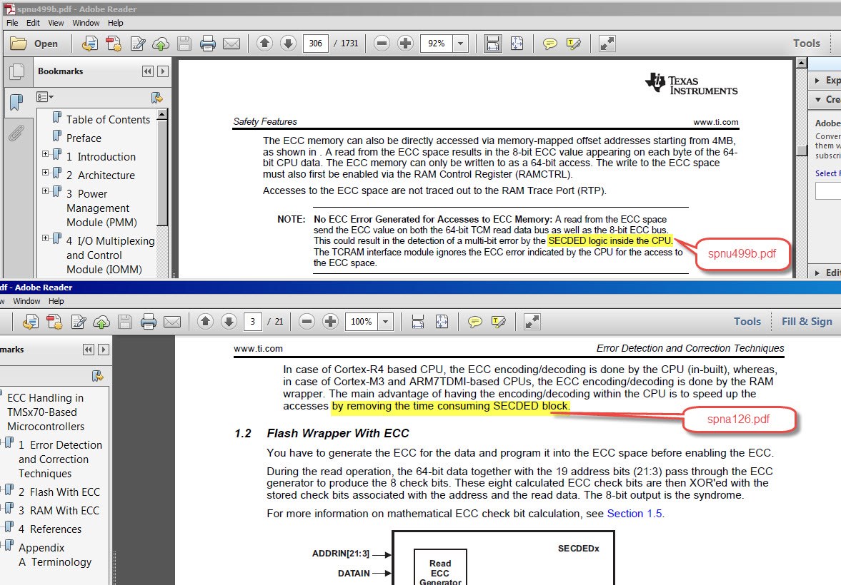
In the spna126.pdf it is mentioned that ECC encoding/decoding logic is resident with Cortex-R4 side and "time consuming SECDED Logic is in the Flash Wrapper".
In spnu499b.pdf, it is mentioned that SECDED Logic is inside Cortex-R4.
I have attached the following snippets from the above mentioned document for easier reference.
Can you please explain ECC complete signal chain is divided between Flash Wrapper side and Cortex-R4 side?
I am assuming it consists of following sub-blocks:
ECC Encoding Logic -- For k bit data it produces n-k bits of ECC
ECC Decoding Logic -- For n bit input, it calculates n-k bits of ECC
SECDED Logic for Error Detection -- Detects if there is more than one bit error and if it is only one bit error then it corrects it
Thank you.
Regards
Pashan
Hi Pashan,
Which device are your referring to? You are quoting from the below statements in spna126.
In case of Cortex-R4 based CPU, the ECC encoding/decoding is done by the CPU (in-built), whereas, in case of Cortex-M3 and ARM7TDMI-based CPUs, the ECC encoding/decoding is done by the RAM wrapper. The main advantage of having the encoding/decoding within the CPU is to speed up the accesses by removing the time consuming SECDED block.
For all Hercules R4 based devices with ATCM and BTCM interfaces they ECC checking is completely done inside the CPU. What is connected to the ATCM is the flash memory excluding the EEprom emulation bank and OTP sectors. What is connected to BTCM is the SRAM. The CPU does all ECC checking for the flash memory (the normal banks such as bank0, bank1) and BTCM (the SRAM). However, for Bank7 (the Emulation flash bank) and the OTP sectors, they are accessed via the CPU's AXI bus interface. The AXI bus interface does not have ECC checking capability. Therefore, the ECC logic is replicated inside the flash wrapper only for accesses to the flash EEprom emulation bank and OTP.
1> Which bits for Cortex-R4 System Register as shown below:
c5, Data Fault Status Register
FSR[10, 3:0] values?
No, as I said the ECC checking for bank7 is done by the flash wrapper rathar than the CPU. So the CPU never knows that the data has been detected with error and been corrected. DFSR register is not updated inside the CPU.
2> Will there be any effect on the following Cortex-R4 System Register as shown below and if yes, which bits:
c5, Auxiliary Fault Status Registers
See answer above.
3> Will there be any other Cortex-R4 System Register Status changes?
If yes, then which one and which bits?
See answer above.
4> ESM Status Register 4 (ESMSR4) -- Bit 3 will be SET --
-- Because -- FMC - correctable error (EEPROM bank access) is connected to Group1 Channel 35
Yes.
5>Flash Wrapper -- FCOR_ERR_CNT Flash Correctable Error Count Register content will be incremented by 1
No, it will be the EE_COR_ERR_ADD at offset 0x310
6>Flash Wrapper -- FCOR_ERR_ADD Flash Correctable Error Address Register will contain 0xF008E3F0
No, it should be the EE_COR_ERR_POS
7>Flash Wrapper -- FCOR_ERR_POS Flash Correctable Error Position Register will have Bit 0 SET
No, it should be the EE_COR_ERR_POS and if bit0 is the bit that is detected for single bit error.
8> Flash Wrapper -- FEDACSTATUS Flash Error Detection and Correction Status Register
-- Bit 16 will be SET
-- -- Bit 1 if EZFEN bit is SET
No, should be the EE_STATUS at 0x31C
Please answer below every question with your comments.
Assume CPSR Register I and F bits are SET, which means no ESM Interrupts will be taken.
Are you asking a general question here. If the I and F bits are set then the CPU does not take interrupt. Note that once the F bit is cleared it can not be set again until a reset.
May be in your answer you can add corresponding bit changes for 32-Bit read from 0xF008E3FC [for Double Bit ECC Selftest on Bus 2] in a separate paragraph under respective questions. Or, I can ask you in the next phase.
For unncorrectable error the bit 8 in the EE_STATUS will be set.
9> Cortex-R4 will not take ABORT Vector for Bus 2 Double Bit ECC Error during 32-Bit Read from 0xF008E3FC.
Is that the correct statement?
No abort will be taken because the AXI does not do any ECC checking. It has no understanding what is going with the quality of the data read on the AXI bus. For ATCM/BTCM, all 2bit uncorrectable ECC error will result in abort.
Please note I will be out of office for a few days. Please expect delayed repsonse.