This thread has been locked.
If you have a related question, please click the "Ask a related question" button in the top right corner. The newly created question will be automatically linked to this question.
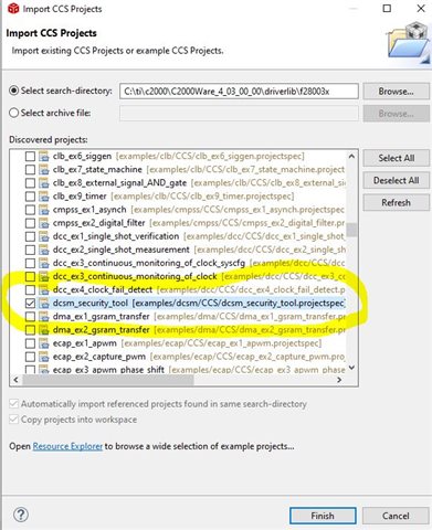
We are developing a new prototype using the TMS320F280034PM (64 pin version). As a basic test on the new board, we imported an example sysconfig project for this part which just toggles a GPIO. The project is 'gpio_ex2_toggle' and we just changed the GPIO pin allocation in sysconfig to drive on of our board LEDs.
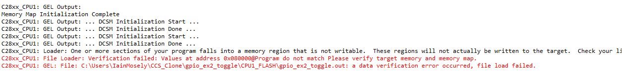
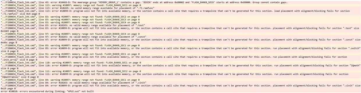
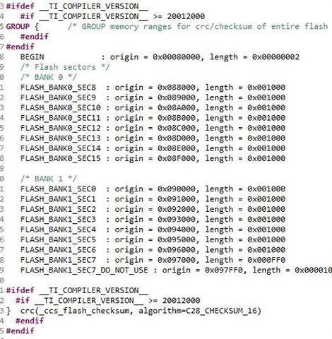
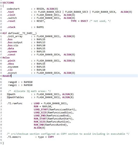
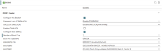
The default project settings place the program in RAM and when we run a debug session with these settings, everything works and the LED on our board blinks correctly. We wanted to make sure that we can also program flash so we changed the project settings to use 'CPU1_FLASH' which now calls up the 280003x_generic_flash_lnk.cmd linker file. When we try to build and debug the project, the build executes correctly but we get an error when the debug session tries to start:-
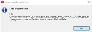
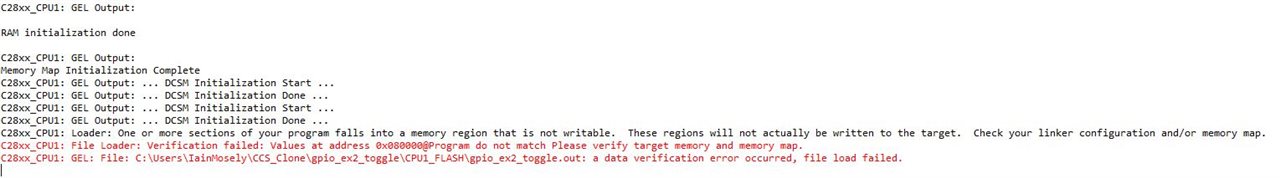
Looking at the console output at this point, we see a bit more detail on the error:-
Are there some extra configuration settings which CCS needs to be able to program flash on this device?
Many Thanks,
Iain
Hi Lain,
Please use CCS Version: 12.5.0. Let us know if that does not fix your issue.
Thanks and regards,
Vamsi
Hi Vamsi,
I am currently using Version: 11.2.0.00007 so will update to the latest and let you know if this solves the issue.
Many Thanks,
Iain
Hi folks, I just updated to the latest version of CCS and sysconfig. CCS version is 12.5.0.00007 and sysconfig is release 1.18.0.
At the moment, this hasn't fixed the issue, I still get the memory verification error, see below. I am using the 280003x_generic_flash_lnk.cmd file presently - is this the correct one to use?
Hi Lain,
The error shows that you are using the address 0x80000 in your linker command file. This address is not valid for F280034.
I will check with our team to see if we have a F280034 specific linker command file that you can use.
I will get back to you in a day or two.
Thanks and regards,
Vamsi
Hi Lain,
Could you use the F280034_flash_lnk.cmd provided as part of the CCS installation?
Path: \ti\ccs1240\ccs\ccs_base\c2000\include
Thanks and regards,
Vamsi
Hi Vamsi,
I tried the F280034_flash_lnk.cmd file at that location in CCS (i have version 12.5 though) but still get errors when linking. Here is what the errors indicate:-
I took a look at the CMD file to try to understand what the errors might be and at least the first one seems to be around a discontinuity in the group memory range between the 'begin' location and the first set of Flash (FLASH_BANK0_SEC8). Also, under the 'SECTION' part of the file, several regions of memory are referenced which aren't defined in the 'MEMORY' part of the file. The 280034 part appears not to have Sectors 0 to 7 defined in BANK 0 which is confirmed when I look at the memory map of the device in the datasheet. Is this CMD file correct or am I misunderstanding something here?
Thanks,
Iain
Lain,
Yes, the first half of the Bank0 is not available in F280034 device.
Are you saying that the linker command file has those memories defined in it?
Thanks and regards,
Vamsi
Hi Vamsi, yes, the F280034_flash_lnk.cmd file defines the two flash banks, FLASH_BANK0_SEC8 to 15 and FLASH_BANK1_SEC0 to 7:-
I think this is correct as it matches the memory map in the F290034 datasheet. However, the same F280034_flash_lnk.cmd file then tries to reference undefined flash sections in the 'Sections' part of the file. Below you can see that it tries to reference sections such as FLASH_BANK0_SEC1 which I don't think is correct.
I might be misunderstanding how these linker files work but I would have thought the 'sections'part can only call up regions of memory already explicitly defined in the 'memory' section?
Please can you check on this for me as I'm still not able to compile to flash on this part.
Many Thanks, Iain
Hi Lain,
Yes, I reviewed it - it is a bug. I will file a jira and notify the team that generated it.
For your application purpose - you can use the memories that you seem fit for your application (please replace invalid sectors with valid sectors in the Sections part of the linker command file.
Thanks and regards,
Vamsi
Thanks Vamsi. I'll make the changes that I think need to be made and let you know how it goes.
Hi Vamsi, I modified the linker file as below and can now program the flash. In addition to updating the memory sections called up in the 'Sections' part, I also needed to modify the Begin Address to be the start of FLASH_BANK0_SEC8 (i.e. 0x88000) and the start/length of FLASH_BANK0_SEC8. Please could you check to see if these make sense? I can program flash now but the program does not appear to run when I cycle power so maybe I have misplaced the Begin address?
/* //########################################################################### // // FILE: F280034_flash_lnk.cmd // // TITLE: Linker Command File For F280034 Device // //########################################################################### */ MEMORY { BOOT_RSVD : origin = 0x00000002, length = 0x00000126 RAMM0 : origin = 0x00000128, length = 0x000002D8 RAMM1 : origin = 0x00000400, length = 0x000003F8 /* on-chip RAM block M1 */ // RAMM1_RSVD : origin = 0x000007F8, length = 0x00000008 /* Reserve and do not use for code as per the errata advisory "Memory: Prefetching Beyond Valid Memory" */ RAMLS0 : origin = 0x00008000, length = 0x00000800 RAMLS1 : origin = 0x00008800, length = 0x00000800 RAMLS2 : origin = 0x00009000, length = 0x00000800 RAMLS3 : origin = 0x00009800, length = 0x00000800 RAMLS4 : origin = 0x0000A000, length = 0x00000800 RAMLS5 : origin = 0x0000A800, length = 0x00000800 RAMLS6 : origin = 0x0000B000, length = 0x00000800 RAMLS7 : origin = 0x0000B800, length = 0x00000800 /* Combining all the LS RAMs */ //RAMLS : origin = 0x00008000, length = 0x00004000 RAMGS0 : origin = 0x0000C000, length = 0x00001000 RAMGS1 : origin = 0x0000D000, length = 0x00001000 RAMGS2 : origin = 0x0000E000, length = 0x00001000 RAMGS3 : origin = 0x0000F000, length = 0x00000FF8 // RAMGS3_RSVD : origin = 0x000FFF8, length = 0x00000008 /* Reserve and do not use for code as per the errata advisory "Memory: Prefetching Beyond Valid Memory" */ BOOTROM : origin = 0x003F8000, length = 0x00007FC0 SECURE_ROM : origin = 0x003F2000, length = 0x00006000 RESET : origin = 0x003FFFC0, length = 0x00000002 #ifdef __TI_COMPILER_VERSION__ #if __TI_COMPILER_VERSION__ >= 20012000 GROUP { /* GROUP memory ranges for crc/checksum of entire flash */ #endif #endif BEGIN : origin = 0x00088000, length = 0x00000002 /* Flash sectors */ /* BANK 0 */ FLASH_BANK0_SEC8 : origin = 0x088002, length = 0x000FFE FLASH_BANK0_SEC9 : origin = 0x089000, length = 0x001000 FLASH_BANK0_SEC10 : origin = 0x08A000, length = 0x001000 FLASH_BANK0_SEC11 : origin = 0x08B000, length = 0x001000 FLASH_BANK0_SEC12 : origin = 0x08C000, length = 0x001000 FLASH_BANK0_SEC13 : origin = 0x08D000, length = 0x001000 FLASH_BANK0_SEC14 : origin = 0x08E000, length = 0x001000 FLASH_BANK0_SEC15 : origin = 0x08F000, length = 0x001000 /* BANK 1 */ FLASH_BANK1_SEC0 : origin = 0x090000, length = 0x001000 FLASH_BANK1_SEC1 : origin = 0x091000, length = 0x001000 FLASH_BANK1_SEC2 : origin = 0x092000, length = 0x001000 FLASH_BANK1_SEC3 : origin = 0x093000, length = 0x001000 FLASH_BANK1_SEC4 : origin = 0x094000, length = 0x001000 FLASH_BANK1_SEC5 : origin = 0x095000, length = 0x001000 FLASH_BANK1_SEC6 : origin = 0x096000, length = 0x001000 FLASH_BANK1_SEC7 : origin = 0x097000, length = 0x000FF0 FLASH_BANK1_SEC7_DO_NOT_USE : origin = 0x097FF0, length = 0x000010 /* Reserve and do not use for code as per the errata advisory "Memory: Prefetching Beyond Valid Memory" */ #ifdef __TI_COMPILER_VERSION__ #if __TI_COMPILER_VERSION__ >= 20012000 } crc(_ccs_flash_checksum, algorithm=C28_CHECKSUM_16) #endif #endif } SECTIONS { codestart : > BEGIN, ALIGN(8) .text : >> FLASH_BANK0_SEC10 | FLASH_BANK0_SEC11 | FLASH_BANK0_SEC12, ALIGN(8) .cinit : > FLASH_BANK0_SEC9, ALIGN(8) .switch : > FLASH_BANK0_SEC9, ALIGN(8) .reset : > RESET, TYPE = DSECT /* not used, */ .stack : > RAMM1 #if defined(__TI_EABI__) .init_array : > FLASH_BANK0_SEC9, ALIGN(8) .bss : > RAMLS5 .bss:output : > RAMLS3 .bss:cio : > RAMLS0 .data : > RAMLS5 .sysmem : > RAMLS5 .const : > FLASH_BANK0_SEC12, ALIGN(8) #else .pinit : > FLASH_BANK0_SEC9, ALIGN(8) .ebss : > RAMLS5 .esysmem : > RAMLS5 .cio : > RAMLS0 .econst : > FLASH_BANK0_SEC12, ALIGN(8) #endif ramgs0 : > RAMGS0 ramgs1 : > RAMGS0 /* Allocate IQ math areas: */ IQmath : > FLASH_BANK0_SEC9, ALIGN(8) IQmathTables : > FLASH_BANK0_SEC10, ALIGN(8) .TI.ramfunc : LOAD = FLASH_BANK0_SEC9, RUN = RAMLS0, LOAD_START(RamfuncsLoadStart), LOAD_SIZE(RamfuncsLoadSize), LOAD_END(RamfuncsLoadEnd), RUN_START(RamfuncsRunStart), RUN_SIZE(RamfuncsRunSize), RUN_END(RamfuncsRunEnd), ALIGN(8) /* crc/checksum section configured as COPY section to avoid including in executable */ .TI.memcrc : type = COPY } /* //########################################################################### // End of file. //########################################################################### */
Hi Lian,
Do you mean to say that the application did not execute in standalone mode without the debugger?
How are the boot mode GPIOs configured? If not already, try the flash boot mode.
Thanks and regards,
Vamsi
Hi Vamsi, unfortunately not. I can program the flash now and with the debugger connected can start the application running. However, if I remove the debugger and re-cycle power then execution does not start. The boot0 and boot1 pins are both tied high on our board via 10k resistors which should allow the unit to boot from flash.
Please can you check the setup of the code sections in the linker file I attached above which control the location of where code execution begins (or maybe the reset vector?) I'm still learning about how these linker files work so not sure if that part is correct yet.
Thanks, Iain
Hi Lian,
I reviewed the TRM (see below snap) - On this device, BOOTDEFx has to be programmed with below highlighted value for the entry point that you want to use.
Thanks and regards,
Vamsi
Thanks Vamsi,
OK, I found the section in the 280034 datasheet too and have programmed the BOOTDEF1,2,3,4 registers to all start from the 0x00088000 address. This has solved the problem now our custom board can now boot in standalone mode. Thanks very much for your help.
Best wishes, Iain
Hi Iain,
I have been struggling with exactly the same issue as this, on the same device. I got as far as now flashing the device but am unsure on how to set the BOOTDEF registers. Could you advise how to do that?
Once they have been set does this mean other boot modes such as SCI won't work?
Thanks,
Alex
Hi Alex, I did this by importing the 'dcsm_security_tool' example project:-
I opened the dcsm_security_tool.syscfg file and this allows you to configure the BOOTDEFx registers when you tick the 'Configure Boot Setting' box under DCSM0. I set the BOOTDEF parameters I needed and then when you compile and flash this program, the one time registers get set. You can then close this project and re-flash your own project - it should work then. be careful with BOOTDEFx registers, these and the Boot pins are all one time programmable so if you get it wrong, you will need to replace the processor! There may be an easier way to do this but this is what I did.
I haven't looked further into the impact of this on the other boot modes, let us know how you get on.
Thanks, Iain
Hi Iain,
Thanks for those clear instructions, that works for me now.
I also set BOOTDEF1,2,3,4 to point to the correct flash address. When I have more boards assembled I may try setting just BOOTDEF1 for flash and another to enable SCI boot. The boot mode select pins should then control which mode to use. Right now all roads lead to flash!
Alex
Following up on this. If BOOTDEF1,2,3,4 are all set to the flash entry point then no other boot options will be available on the device. In my case I wanted boot from flash as default but also the option to boot from SCI to enable over-the-air updates. See the configuration below that I used.
I only needed to use one boot pin (GPIO24 in my case). I set BOOTDEF1 to the flash entry point, which is used when GPIO24 is at it's default high level. I set BOOTDEF0 (GPIO24 = low) to be the SCI boot, using the SCI GPIO specified.
Thanks for pointing me to this, and particulally the sysconfig setup. It makes things much eaiser.
I read in the manual that there are emulation equivalents for BOOTDEF for debugging purposes, which allow one to play around without writing to the OTP registers. I didn't try this though.
Cheers!
Alex
Thanks Alex, great to hear about this. I haven't tried to boot from anything other than flash presently but it is on my todo list and with your info I have a good chance of it working. Many Thanks,