This thread has been locked.

If you have a related question, please click the "Ask a related question" button in the top right corner. The newly created question will be automatically linked to this question.

TMS320F280049C: SPI STE signal problem

Part Number: TMS320F280049C
Other Parts Discussed in Thread: SYSCONFIG, C2000WARE

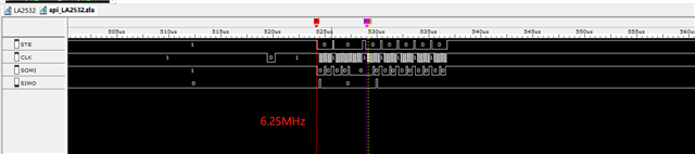
when baudrate set to 3.125MHz or 1MHz, use fifo mode set the delay between fifo to shift register to 0, the STE remain low in the whole process

when buadrate up to 6.25Mhz or 12.5MHz, STE will back to high for a few spi cycle, this coud affect data back on the SOMI line, how can i solve it

  • sysconfig configuration

    trsaction function SPI_PollingFIFOTransaction

  • Hi Nirvana Xun,

    It's a bit unclear to me what the issue is here. Are you saying that when you increase SPI speed to 12.5MHz, you see corrupt data reads/transmits? Is your system still reading/writing data correctly? Or is the question only about the SPISTE line activity?

    Could you also please explain the nature of your application - what is the desired SPI usage (i.e. what type of data/size/how many characters are you trying to send/receive and what device are you communicating with?)?

    Best Regards,

    Allison

  • i used SPI to communicate with a network module, sent 0x80 0x00 0x00 0x04 0x00 0x00 0x00 0x00 to read a chip cookie from the module

    in the first diagram the STE stayed low during the whole SPI process, the slave module answered the master's inquiry correctly, SPI baudrate was below 5Mbps

    in the second and third diagram, i promoted the speed up to 6.25Mbps and 12.5Mbps, the STE signal could not maintain low in the communication, when this signal got to high in a communicating process, the slave thought the communication start again and could not answer the sequence properly. i had already set the fifo to buffer delay to "0", there is no other interrupt running , how can i solve it

  • Hi Nirvana Xun, 

    How are you transmitting the data (i.e. how/when are you writing to the TXBUF and how many bytes of data at a time?)? If the only thing that changes the activity of SPISTE between diagrams 1, 2, and 3 is the speed of your SPI (and depending on how you are writing to TXBUF), then this appears to be inherent to the SPI timing specifications. Here is some explanation of what I am speculating:

    • When you use the default SPISTE pin as your chip select (rather than manually using a GPIO as a chip select), the SPI module will toggle the SPISTE line on its own.
    • The the timings of when the SPISTE is considered to be active (valid) versus when it is no longer active (invalid) are outlined in the device datasheet, and the important thing to note is that these timing specifications vary depending on the speed you are operating SPI at.
    • For example, if you are operating master mode (and non-high-speed mode) with clock phase = 0, the datasheet table would be:
      • And in particular, you would be interested in number 24:
      • This is visualized in the corresponding figure from the datasheet (see parameter #24 in the image below):
        • Note that the figure above also has a footnote stating that on the trailing end of the word, SPISTE will go inactive except between back-to-back transmit words in both FIFO and non-FIFO modes. 

    So to sum up, to me it appears that this behavior of SPISTE is expected - the only caveat is that you have to be sure that the device you are communicating with is okay with this behavior. If the other device is expecting SPISTE to remain low through the entire time (even between each data), then there will be issues with communication (but there are ways to work around this by instead manually controlling the chip select using a regular GPIO rather than the default SPISTE). The expected SPI communication information should be given in the other device datasheet.

    Let me know if the above makes sense and/or if you have conflicting findings.Slight smile

    Best Regards,

    Allison

  • the transmit function was "SPI_PollingFIFOTransaction" provided by Dirverlib, i think this function uses FIFO mode, but i don't know whether it has used back-to-back transmit scheme, i did set the delay to zero and i cannot find a register bit to control STE.

    anyway, in diagram 2 and 3, although i used a GPIO pin to drive STE, the CLK signal was not consecutive, still not able to get proper answer.

    this is the datasheet of slave module

    just let me know how to keep STE effective in one communication frame when the speed is above 5MHz

  • Hi Nirvana Xun,

    Looks like the other device is expecting a constantly active SPISTE (SPISTE is active low, so we want it to remain low for the full transmission). We can ensure it remains low by controlling it manually by using a GPIO rather than the dedicated SPISTE signal. There are unfortunately no specific examples to showcase this setup, but it is mentioned in the TRM which I will also try to explain differently to clarify: 

    Typically, a dedicated SPISTE pin ("SPI Slave Transmit-Enable" pin)- also called a CS pin ("Chip Select" pin)- is used to select which slave is 'active' at a certain time. A specific slave is considered 'active' when its SPISTE pin is pulled low, which allows for the slave to receive data. In some cases, there are limited dedicated SPISTE signals/pins available on devices. Thus, if you would like to emulate more slaves then you can use other GPIOs to act as SPISTE pins (one GPIO/SPISTE per slave). In your case, you simply want to control the SPISTE to cater to the other device you are communicating with.

    In either case, to do this, you have to set the configuration of the GPIO signal to be an 'output' that way the digital signal output from the GPIO module can be used to select active slaves. So before any data can be sent to the slave, you would have the master device (as we are in master mode) pull the specific slave's GPIO (acting as the SPISTE) output low to allow that slave to receive data. Note that this GPIO would be controlled by using settings and functions of the GPIO control registers. 

    Hope this helps, and please let me know if you need further clarification on this.

    Best Regards,

    Allison

  • in the second and third diagram, the CLK signal was also not consecutive during tansmission. although i can use GPIO, CLK signal will affect the slave to receive correct data. this may not work as well.

  • Hi Nirvana Xun,

    If you are only needing to transmit 8 words, you should be able to do so back to back since the FIFOs are 16 levels deep (plenty of space to write 8 words to the TXFIFO and without needing to wait for space).

    How are you currently sending/receiving your data? Are you using interrupts in your application? If you haven't already, please be sure to review some of our C2000Ware examples that utilize FIFO mode and let me know if you are able to implement them in you code. (such as spi_ex2_loopback_fifo_interrupts or spi_ex4_external_loopback_fifo_interrupts from the C2000Ware DriverLib examples located at {C2000Ware}\driverlib\f28004x\examples\spi).

    Best Regards,

    Allison

  • the communication tests were only hardware test, in normal operation, it needs to transfer a much longer frame to slave module, up to 1000 bytes

    i used SPI_PollingFIFOTransaction function to transfer data, so the fifo was used and the delay between FIFO to shift register was zero

  • Hi Nirvana Xun,

    Have you referenced some of the C2000Ware examples I mentioned that use FIFO or tried any other methods of SPI communication besides the polling FIFO function? If not, these could be very helpful to leverage. It might also be useful to try using other APIs (e.g. SPI_writeDataBlockingFIFO, SPI_readDataBlockingFIFO, etc.) to see if the timing behavior changes.

    To clarify, are you getting specific errors/having trouble with your SPI communication between devices (slave/peripheral device is getting errors or bad data due to the timing)?

    Best Regards,

    Allison