Other Parts Discussed in Thread: CONTROLSUITE
Hello Team,
I am using F28069F microcontroller, with the customized board, I am facing problems with understanding the ADC module conversion.
I will post my findings, requesting to help me with this.
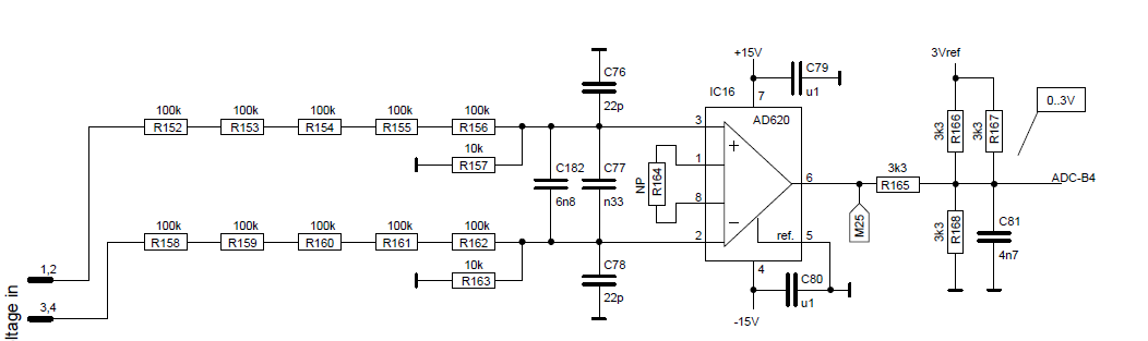
In the board I am using AD620 is used for the conversion.
I applied input voltage between the two terminals of the AD620, I have following output in the ADCRESULT register.
Input voltage | ADCRESULT register value (decimal format)
-20 V | 1880
-15 V | 1920
-10 V |1955
-5 V | 1990
0 V | 2020
5 V | 2054
10 V | 2085
15 V | 212
20 V | 2150.
from the values obatined above I can see the variation of approximate 30 decimal increment\decrement in ADC result register value.
I followed the procedure in the following post ( ) for relation between the ADC digital output and analog input.
Vin = Output code * LSB Size.
LSB Size = FSR/(2^N).
#define USER_ADC_FULL_SCALE_VOLTAGE_V (612.0)
#define USER_IQ_FULL_SCALE_VOLTAGE_V (350.0)
Using the FSR = 612 and 12 bit ADC core.
2^12 = 4096 bits.
LSB size = 0.1494.
Output code = (Input voltage)/(LSB size).
Input voltage = 5V
Output code = 34.
ADCRESULTREGISTER value = 2020 +34 = 2054.
same procedure for input voltage = -5V, will give output code of -34.
ADCRESULTREGISTER value = 2020 - 34 = 1990.
Requesting to correct me if I am wrong, in the way it is calculated.
I have also attached the ADC circuit used for conversion.
Thanks and best regards,
Chetan.