This thread has been locked.
If you have a related question, please click the "Ask a related question" button in the top right corner. The newly created question will be automatically linked to this question.
Tool/software: Code Composer Studio
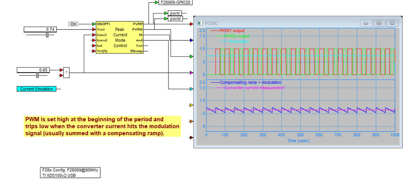
Hello everyone, i'm doing a current programmed mode for my SEPIC converter control. I'd like to know how to do it using the ramp generator and the comparator block of the target.
I tried doing the next code but the signal in the oscilloscope is 100 kHz 99% duty cycle. I'd like to get a 50% duty cycle signal. Thanks for your time
#include "DSP28x_Project.h" // Device Headerfile and Examples Include File
#include <stdint.h>
#include <stdbool.h>
//f deseada en kHz
float f=100;
float period=90000/100;
float Toff;
float h;
float vo;
float io;
float ip;
float vp;
float VP=0;
float IO=0;
float IP=0;
float VO=0;
int contador=0;
float Kp=0.2990;
float Ki=676.7921;
float Tm=1/100000;
float Vref=0;
float SalPI[2];
float EntPI[2];
float ACW;
// Prototype statements for functions found within this file.
void Adc_Config(void);
void InitEPwm2(void);
void InitEPwm2Gpio(void);
main()
{
InitSysCtrl();
InitEPwm2Gpio();
DINT;
InitPieCtrl();
IER = 0x0000;
IFR = 0x0000;
InitPieVectTable();
EALLOW; // This is needed to write to EALLOW protected register
EDIS; // This is needed to disable write to EALLOW protected registers
InitAdc(); // For this example, init the ADC
AdcOffsetSelfCal();
IER |= M_INT14;
PieCtrlRegs.PIEIER1.bit.INTx7 = 1;
EINT; // Enable Global interrupt INTM
ERTM; // Enable Global realtime interrupt DBGM
// Configure GPIO
EALLOW;
GpioCtrlRegs.GPAPUD.bit.GPIO0 = 1; // Disable pull-up on GPIO0 (EPWM1A)
GpioCtrlRegs.GPAPUD.bit.GPIO1 = 1; // Disable pull-up on GPIO1 (EPWM1B)
GpioCtrlRegs.GPAMUX1.bit.GPIO0 = 1; // Configure GPIO0 as EPWM1A
GpioCtrlRegs.GPAMUX1.bit.GPIO1 = 1; // Configure GPIO1 as EPWM1B
GpioCtrlRegs.GPAPUD.bit.GPIO2 = 1; // Disable pull-up on GPIO2 (EPWM2A)
GpioCtrlRegs.GPAPUD.bit.GPIO3 = 1; // Disable pull-up on GPIO3 (EPWM2B)
GpioCtrlRegs.GPAMUX1.bit.GPIO2 = 1; // Configure GPIO2 as EPWM2A
GpioCtrlRegs.GPAMUX1.bit.GPIO3 = 1; // Configure GPIO3 as EPWM2B
GpioCtrlRegs.GPAPUD.bit.GPIO4 = 1; // Disable pull-up on GPIO4 (EPWM3A)
GpioCtrlRegs.GPAPUD.bit.GPIO5 = 1; // Disable pull-up on GPIO5 (EPWM3B)
GpioCtrlRegs.GPAMUX1.bit.GPIO4 = 0; // Configure GPIO4 as EPWM3A
GpioCtrlRegs.GPAMUX1.bit.GPIO5 = 0; // Configure GPIO5 as EPWM3B
GpioCtrlRegs.GPADIR.bit.GPIO4 = 1;
GpioCtrlRegs.GPADIR.bit.GPIO5 = 1;
GpioCtrlRegs.GPAPUD.bit.GPIO8 = 1; // Disable pull-up on GPIO8 (EPWM5A)
GpioCtrlRegs.GPAMUX1.bit.GPIO8 = 1; // Configure GPIO1 as EPWM5A
GpioCtrlRegs.GPBPUD.bit.GPIO32 = 0;
GpioCtrlRegs.GPBMUX1.bit.GPIO32 = 2;
// Configure GPIO31 as a GPIO output pin (Evalkit Blue LED)
GpioCtrlRegs.GPAMUX2.bit.GPIO31 = 0;
GpioCtrlRegs.GPADIR.bit.GPIO31 = 1;
// RED OCP LED
GpioCtrlRegs.GPBMUX1.bit.GPIO34 = 0;
GpioCtrlRegs.GPBDIR.bit.GPIO34 = 1;
// GPIO 10 as input (ENABLE SWITCH)
GpioCtrlRegs.GPAPUD.bit.GPIO10 = 1; // Disable pullup on GPIO10
GpioCtrlRegs.GPAMUX1.bit.GPIO10 = 0; // GPIO10 = GPIO10
GpioCtrlRegs.GPADIR.bit.GPIO10 = 0; // GPIO10 = input
GpioCtrlRegs.GPACTRL.bit.QUALPRD1=10; // Qual period = SYSCLKOUT/10
GpioCtrlRegs.GPAQSEL1.bit.GPIO10=2; // 6 samples
AdcRegs.ADCCTL1.bit.ADCBGPWD = 1; // Power ADC BandGap
AdcRegs.ADCCTL1.bit.ADCREFPWD = 1; // Power reference
AdcRegs.ADCCTL1.bit.ADCPWDN = 1; // Power ADC
AdcRegs.ADCCTL1.bit.ADCENABLE = 1; // Enable ADC
AdcRegs.ADCCTL1.bit.ADCREFSEL = 0; // Select internal BandGap
EDIS;
InitEPwm2();
PieCtrlRegs.PIEIER1.bit.INTx7 = 1;
// Enable EPWM INTn in the PIE: Group 2 interrupt 1
PieCtrlRegs.PIEIER2.bit.INTx1 = 1;
// Enable EPWM1_INT in the PIE: Group 3 interrupt 1
PieCtrlRegs.PIEIER3.bit.INTx1 = 1;
// Enable EPWM2_INT in the PIE: Group 3 interrupt 2
PieCtrlRegs.PIEIER3.bit.INTx2 = 1;
// Enable EPWM4_INT in the PIE: Group 3 interrupt 4
PieCtrlRegs.PIEIER3.bit.INTx4 = 1;
//Enable ADC in the PIE: Group 1
PieCtrlRegs.PIEIER1.bit.INTx1 = 1; // Enable INT 1.1 in the PIE
// Enable global Interrupts and higher priority real-time debug events:
PieCtrlRegs.PIEACK.all = 0xFFFF;
// Wait for ADC interrupt
}
void InitEPwm2Gpio(void)
{
EALLOW;
/* Disable internal pull-up for the selected output pins
for reduced power consumption */
// Pull-ups can be enabled or disabled by the user.
// This will enable the pullups for the specified pins.
// Comment out other unwanted lines.
GpioCtrlRegs.GPAPUD.bit.GPIO2 = 1; // Disable pull-up on GPIO2 (EPWM2A)
GpioCtrlRegs.GPAPUD.bit.GPIO3 = 1; // Disable pull-up on GPIO3 (EPWM2B)
/* Configure EPwm-2 pins using GPIO regs*/
// This specifies which of the possible GPIO pins will be EPWM2 functional pins.
// Comment out other unwanted lines.
GpioCtrlRegs.GPAMUX1.bit.GPIO2 = 1; // Configure GPIO2 as EPWM2A
GpioCtrlRegs.GPAMUX1.bit.GPIO3 = 1; // Configure GPIO3 as EPWM2B
EDIS;
}
void InitEPwm2()
{
EALLOW;
//Fórmula 40Mhz/50kHz=800period in TBCLK counts
EPwm1Regs.TBPRD = period;
//EPwm1Regs.TBPHS.half.TBPHS = 0;
//EPwm1Regs.TBPHS = 0x0000; // Set Phase register to zero
EPwm1Regs.TBPHS.half.TBPHS = 0; // Set Phase register to zero
EPwm1Regs.TBCTR = 0; // clear TB counter
EPwm1Regs.TBCTL.bit.CTRMODE = TB_COUNT_UP;
EPwm1Regs.TBCTL.bit.PHSEN = TB_DISABLE; // Phase loading disabled
EPwm1Regs.TBCTL.bit.SYNCOSEL = TB_SYNC_DISABLE;
EPwm1Regs.TBCTL.bit.PRDLD = TB_SHADOW;
EPwm1Regs.TBCTL.bit.HSPCLKDIV = TB_DIV1; // TBCLK = SYSCLK
EPwm1Regs.TBCTL.bit.CLKDIV = TB_DIV1;
EPwm1Regs.CMPCTL.bit.SHDWAMODE = CC_SHADOW;
EPwm1Regs.CMPCTL.bit.SHDWBMODE = CC_SHADOW;
EPwm1Regs.CMPCTL.bit.LOADAMODE = CC_CTR_ZERO; // load on CTR = Zero
EPwm1Regs.CMPCTL.bit.LOADBMODE = CC_CTR_ZERO; // load on CTR = Zero
EPwm1Regs.AQCTLA.bit.ZRO = AQ_SET;
EPwm1Regs.AQCTLA.bit.CAU = AQ_CLEAR;
EPwm1Regs.AQCTLB.bit.ZRO = AQ_SET;
EPwm1Regs.AQCTLB.bit.CBU = AQ_CLEAR;
EPwm1Regs.AQCTLA.bit.PRD = AQ_CLEAR;
EPwm1Regs.AQCTLA.bit.CAU = AQ_SET;
//
// Run Time
// = = = = = = = = = = = = = = = = = = = = = = = =
//EPwm1Regs.CMPA.half.CMPA = 0.5; // adjust duty for output EPWM1A
Comp1Regs.COMPCTL.bit.COMPDACEN = 1;
Comp1Regs.COMPCTL.bit.SYNCSEL = 1;
Comp1Regs.COMPCTL.bit.CMPINV = DC_BLANK_NOTINV;
Comp1Regs.COMPCTL.bit.COMPSOURCE = 0;
Comp1Regs.COMPCTL.bit.QUALSEL = 0;
Comp1Regs.DACCTL.bit.RAMPSOURCE = 0;
Comp1Regs.DACCTL.bit.DACSOURCE = 1;
Comp1Regs.DACCTL.bit.FREE_SOFT = 0;
Comp1Regs.DACVAL.all = 1024;
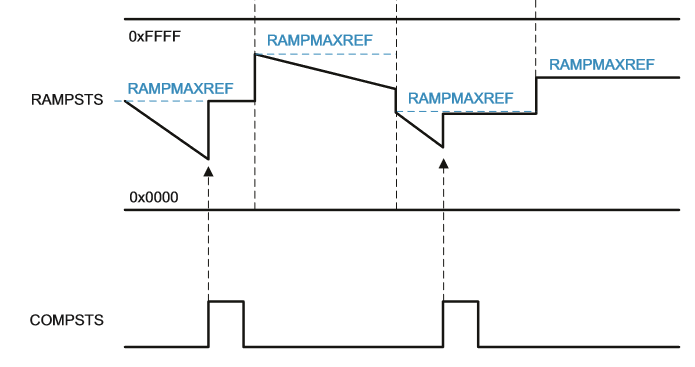
Comp1Regs.RAMPDECVAL_SHDW = 20000;
Comp1Regs.RAMPMAXREF_SHDW = 49000;
Comp1Regs.DACVAL.bit.DACVAL=310;
EPwm1Regs.DCTRIPSEL.bit.DCAHCOMPSEL=0; // DCAH = Comparator output
EPwm1Regs.DCTRIPSEL.bit.DCALCOMPSEL=8;
EPwm1Regs.TZDCSEL.bit.DCAEVT2 = TZ_DCAH_HI; // DCAEVT2 = (will become active as Comparator output goes high)
EPwm1Regs.DCACTL.bit.EVT2SRCSEL = 1;//DC_EVT2; // DCAEVT2 = DCAEVT2 (not filtered)
EPwm1Regs.DCACTL.bit.EVT2FRCSYNCSEL = 1; // Take sync path
EPwm1Regs.TZSEL.bit.DCAEVT2 = 1;
EPwm1Regs.TZCTL.bit.TZA = TZ_FORCE_HI; // EPWM1A will go low
EPwm1Regs.TZCTL.bit.TZB = TZ_FORCE_LO; // EPWM1A will go low
EPwm1Regs.TZEINT.bit.DCAEVT2 = 1;
EPwm1Regs.DCFCTL.bit.PULSESEL = 0; // Time-base counter equal to zero (TBCTR = 0x0000) - start blank timer
EPwm1Regs.DCFCTL.bit.BLANKINV=0;
EPwm1Regs.DCFCTL.bit.BLANKE=1;
EPwm1Regs.DCFCTL.bit.SRCSEL = 3; // Source Is DCAEVT2 Signal
EPwm1Regs.DCFOFFSET = 0; // no offset
EPwm1Regs.DCFWINDOW = 255; // Blanking window
EDIS;
}
Hi Tommy thanks for your reply. I have tried using vissim software and psim software but still cant see a pwm signal using the ramp generator.
I just want to see a pwm signal just modifying the analog input using the ramp,. something like this picture.
I would appreciate if you have a code that let me do this.
Hello Tommy thank you very much for your fast reply, i have been looking and testing that example but the result is not the desired, i want to configure the DAC at the midpoint value (512) ant the result i want to see is the same as an analog comparator(1 when input A2 is 3.3 and 0 when A2 is 0) but at the beggining i get a 470 Hz PWM signal and when i connect A2 to 0 V , GPIO00 goes high and does not do anymore, could you help me with this? i would appreciate so much
Thank you
(Example run like as follows):
//###########################################################################
// Description:
//! \addtogroup f2806x_example_list
//! <h1>ePWM DC Event Trip Comparator (epwm_dcevent_trip_comp)</h1>
//!
//! In this example ePWM1 is configured for PWM Digital Compare Event
//! Trip using Comparator1A and comparator1B pin inputs.
//! DCAEVT1, DCBEVT1 events are triggered by increasing the voltage on
//! COMP1B pin to be higher than that of COMP1A pin.
//! In this example:
//! - ePWM1 has DCAEVT1 and DCBEVT1 as one shot trip sources
//! DCAEVT1 will pull EPWM1A high
//! DCBEVT1 will pull EPWM1B low
//!
//! Initially make the voltage level at COMP1A to be higher than that of COMP1B.
//! Increase voltage on inverting side of comparator(COMP1B pin) to trigger
//! a DCAEVT1, and DCBEVT1. ePWM1 will react to DCAEVT1 and DCBEVT1 as a 1 shot
//! trip. View the EPWM1A/B waveforms on an oscilloscope to see the effect of
//! the events.
//!
//! \b External \b Connections \n
//! - EPWM1A is on GPIO0
//! - EPWM1B is on GPIO1
//! - COMP1A is on ADCA2
//! - COMP1B is on ADCB2
//! - pull COMP1B to a higher voltage level than COMP1A.
//
//###########################################################################
// $TI Release: F2806x C/C++ Header Files and Peripheral Examples V151 $
// $Release Date: February 2, 2016 $
// $Copyright: Copyright (C) 2011-2016 Texas Instruments Incorporated -
// http://www.ti.com/ ALL RIGHTS RESERVED $
//###########################################################################
#include "DSP28x_Project.h" // Device Headerfile and Examples Include File
// Prototype statements for functions found within this file.
void InitEPwm1Example(void);
__interrupt void epwm1_tzint_isr(void);
// Global variables used in this example
Uint32 EPwm1TZIntCount;
Uint32 EPwm2TZIntCount;
void main(void)
{
// Step 1. Initialize System Control:
// PLL, WatchDog, enable Peripheral Clocks
// This example function is found in the F2806x_SysCtrl.c file.
InitSysCtrl();
// Step 2. Initalize GPIO:
// This example function is found in the F2806x_Gpio.c file and
// illustrates how to set the GPIO to it's default state.
// InitGpio(); // Skipped for this example
// For this case just init GPIO pins for ePWM1, ePWM2, and TZ pins
InitEPwm1Gpio();
// Step 3. Clear all interrupts and initialize PIE vector table:
// Disable CPU interrupts
DINT;
// Initialize the PIE control registers to their default state.
// The default state is all PIE interrupts disabled and flags
// are cleared.
// This function is found in the F2806x_PieCtrl.c file.
InitPieCtrl();
// Disable CPU interrupts and clear all CPU interrupt flags:
IER = 0x0000;
IFR = 0x0000;
// Initialize the PIE vector table with pointers to the shell Interrupt
// Service Routines (ISR).
// This will populate the entire table, even if the interrupt
// is not used in this example. This is useful for debug purposes.
// The shell ISR routines are found in F2806x_DefaultIsr.c.
// This function is found in F2806x_PieVect.c.
InitPieVectTable();
// Interrupts that are used in this example are re-mapped to
// ISR functions found within this file.
EALLOW; // This is needed to write to EALLOW protected registers
PieVectTable.EPWM1_TZINT = &epwm1_tzint_isr;
EDIS; // This is needed to disable write to EALLOW protected registers
// Step 4. Initialize all the Device Peripherals:
// This function is found in F2806x_InitPeripherals.c
// InitPeripherals(); // Not required for this example
EALLOW;
SysCtrlRegs.PCLKCR0.bit.ADCENCLK = 1; // Enable Clock to the ADC
AdcRegs.ADCCTL1.bit.ADCBGPWD = 1; // Comparator shares the internal BG reference of the ADC, must be powered even if ADC is unused
DELAY_US(1000); // Delay for Power Up
SysCtrlRegs.PCLKCR3.bit.COMP1ENCLK = 1; // Enable clock to the Comparator 1 block
Comp1Regs.COMPCTL.bit.COMPDACEN = 1; // Power up Comparator 1 locally
Comp1Regs.COMPCTL.bit.COMPSOURCE = 1; // Connect the inverting input to pin COMP1B
////////////////Uncomment following 2 lines to use DAC instead of pin COMP1B //////////////////////////////
Comp1Regs.COMPCTL.bit.COMPSOURCE = 0; // Connect the inverting input to the internal DAC
Comp1Regs.DACCTL.bit.DACSOURCE=0;
Comp1Regs.DACVAL.bit.DACVAL = 512; // Set DAC output to midpoint
///////////////////////////////////////////////////////////////////////////////////////////////////////////
SysCtrlRegs.PCLKCR0.bit.TBCLKSYNC = 0;
EDIS;
InitEPwm1Example();
EALLOW;
SysCtrlRegs.PCLKCR0.bit.TBCLKSYNC = 1;
EDIS;
// Step 5. User specific code, enable interrupts
// Initalize counters:
EPwm1TZIntCount = 0;
// Enable CPU INT3 which is connected to EPWM1-3 INT:
IER |= M_INT2;
// Enable EPWM INTn in the PIE: Group 2 interrupt 1-3
PieCtrlRegs.PIEIER2.bit.INTx1 = 1;
// Enable global Interrupts and higher priority real-time debug events:
EINT; // Enable Global interrupt INTM
ERTM; // Enable Global realtime interrupt DBGM
// Step 6. IDLE loop. Just sit and loop forever (optional):
for(;;)
{
__asm(" NOP");
}
}
__interrupt void epwm1_tzint_isr(void)
{
EPwm1TZIntCount++;
// Leave these flags set so we only take this
// interrupt once
//
// EALLOW;
// EPwm1Regs.TZCLR.bit.OST = 1;
// EPwm1Regs.TZCLR.bit.INT = 1;
// EDIS;
// Acknowledge this interrupt to receive more interrupts from group 2
PieCtrlRegs.PIEACK.all = PIEACK_GROUP2;
}
void InitEPwm1Example()
{
EALLOW;
EPwm1Regs.TBPRD = 6000; // Set timer period
EPwm1Regs.TBPHS.half.TBPHS = 0x0000; // Phase is 0
EPwm1Regs.TBCTR = 0x0000;
// Setup TBCLK
EPwm1Regs.TBCTL.bit.CTRMODE = TB_COUNT_UPDOWN; // Count up/down
EPwm1Regs.TBCTL.bit.PHSEN = TB_DISABLE; // Disable phase loading
EPwm1Regs.TBCTL.bit.HSPCLKDIV = TB_DIV4; // Clock ratio to SYSCLKOUT
EPwm1Regs.TBCTL.bit.CLKDIV = TB_DIV4;
EPwm1Regs.CMPCTL.bit.SHDWAMODE = CC_SHADOW; // Load registers every ZERO
EPwm1Regs.CMPCTL.bit.SHDWBMODE = CC_SHADOW;
EPwm1Regs.CMPCTL.bit.LOADAMODE = CC_CTR_ZERO;
EPwm1Regs.CMPCTL.bit.LOADBMODE = CC_CTR_ZERO;
// Setup compare
EPwm1Regs.CMPA.half.CMPA = 3000;
// Set actions
EPwm1Regs.AQCTLA.bit.CAU = AQ_SET; // Set PWM1A on CAU
EPwm1Regs.AQCTLA.bit.CAD = AQ_CLEAR; // Clear PWM1A on CAD
EPwm1Regs.AQCTLB.bit.CAU = AQ_CLEAR; // Clear PWM1B on CAU
EPwm1Regs.AQCTLB.bit.CAD = AQ_SET; // Set PWM1B on CAD
// Define an event (DCAEVT1) based on TZ1 and TZ2
EPwm1Regs.DCTRIPSEL.bit.DCAHCOMPSEL = DC_COMP1OUT; // DCAH = Comparator 1 output
EPwm1Regs.DCTRIPSEL.bit.DCALCOMPSEL = DC_TZ2; // DCAL = TZ2
EPwm1Regs.TZDCSEL.bit.DCAEVT1 = TZ_DCAH_LOW; // DCAEVT1 = DCAH low(will become active as Comparator output goes low)
EPwm1Regs.DCACTL.bit.EVT1SRCSEL = DC_EVT1; // DCAEVT1 = DCAEVT1 (not filtered)
EPwm1Regs.DCACTL.bit.EVT1FRCSYNCSEL = DC_EVT_ASYNC; // Take async path
// Define an event (DCBEVT1) based on TZ1 and TZ2
EPwm1Regs.DCTRIPSEL.bit.DCBHCOMPSEL = DC_COMP1OUT; // DCBH = Comparator 1 output
EPwm1Regs.DCTRIPSEL.bit.DCBLCOMPSEL = DC_TZ2; // DCAL = TZ2
EPwm1Regs.TZDCSEL.bit.DCBEVT1 = TZ_DCBH_LOW; // DCBEVT1 = (will become active as Comparator output goes low)
EPwm1Regs.DCBCTL.bit.EVT1SRCSEL = DC_EVT1; // DCBEVT1 = DCBEVT1 (not filtered)
EPwm1Regs.DCBCTL.bit.EVT1FRCSYNCSEL = DC_EVT_ASYNC; // Take async path
// Enable DCAEVT1 and DCBEVT1 are one shot trip sources
// Note: DCxEVT1 events can be defined as one-shot.
// DCxEVT2 events can be defined as cycle-by-cycle.
EPwm1Regs.TZSEL.bit.DCAEVT1 = 1;
EPwm1Regs.TZSEL.bit.DCBEVT1 = 1;
// What do we want the DCAEVT1 and DCBEVT1 events to do?
// DCAEVTx events can force EPWMxA
// DCBEVTx events can force EPWMxB
EPwm1Regs.TZCTL.bit.TZA = TZ_FORCE_HI; // EPWM1A will go high
EPwm1Regs.TZCTL.bit.TZB = TZ_FORCE_LO; // EPWM1B will go low
// Enable TZ interrupt
EPwm1Regs.TZEINT.bit.OST = 1;
EDIS;
}
//===========================================================================
// No more.
//===========================================================================
Daniel,
It sounds like you are looking for the direct output of Comparator 1. If you look at the GPIO MUX table in the TRM, you can configure the MUX for COMP1OUT on any of the GPIOs where the comparator output is available. So if you change the GPIO1 mux setting from 0b01 (EPWM) to 0b11 (COMP1OUT), you should be able to see the comparator output directly on GPIO1 instead of EPWM1B.
The GPIO0 output is stuck high after trip because the EPWM1A is configured to react to the comparator with a One Shot Trip (OST) that is never cleared. The code to clear the trip state is commented out in epwm1_tzint_isr(). When you implement the ramp generator, you will likely want a Cycle-By-Cycle (CBC) trip instead.
-Tommy
Hello tommy, thanks for your help. now i can use the comparator but cant with the ramp, i want to see my pwm signal but is too small with de rampdecvalue and i have used some values but still cant see for example a 0.99 duty cycle pwm signal. Here is my code, can you check it and tell me why i cant see a good pwm in gpio1? thanks:
#include "DSP28x_Project.h" // Device Headerfile and Examples Include File
void main(void)
{
InitSysCtrl();
DINT;
InitPieCtrl();
IER = 0x0000;
IFR = 0x0000;
InitPieVectTable();
EALLOW;
EPwm1Regs.TBPRD = 903;
EPwm1Regs.CMPA.half.CMPA = 100;
EPwm1Regs.TBPHS.half.TBPHS = 0; // Set Phase register to zero
EPwm1Regs.TBCTR = 0; // clear TB counter
EPwm1Regs.TBCTL.bit.CTRMODE = TB_COUNT_UP; // Asymmetrical mode
EPwm1Regs.TBCTL.bit.PHSEN = TB_DISABLE; // Phase loading disabled
EPwm1Regs.TBCTL.bit.PRDLD = TB_SHADOW;
EPwm1Regs.TBCTL.bit.SYNCOSEL = TB_SYNC_DISABLE;
EPwm1Regs.TBCTL.bit.HSPCLKDIV = TB_DIV1; // TBCLK = SYSCLK
EPwm1Regs.TBCTL.bit.CLKDIV = TB_DIV1;
EPwm1Regs.CMPCTL.bit.SHDWAMODE = CC_SHADOW;
EPwm1Regs.CMPCTL.bit.LOADAMODE = CC_CTR_ZERO; // load on CTR = Zero
EPwm1Regs.AQCTLA.bit.ZRO = AQ_SET; // Set PWM1A on Zero
EPwm1Regs.AQCTLA.bit.CAU = AQ_CLEAR;
SysCtrlRegs.PCLKCR0.bit.ADCENCLK = 1; // Enable Clock to the ADC
AdcRegs.ADCCTL1.bit.ADCBGPWD = 1; // Comparator shares the internal BG reference of the ADC, must be powered even if ADC is unused
DELAY_US(1000); // Delay for Power Up
SysCtrlRegs.PCLKCR3.bit.COMP1ENCLK = 1; // Enable clock to the Comparator 1 block
Comp1Regs.COMPCTL.bit.COMPDACEN = 1; // Power up Comparator 1 locally
//Comp1Regs.COMPCTL.bit.COMPSOURCE = 1; // Pin analogo B
Comp1Regs.COMPCTL.bit.COMPSOURCE = 0; //DAC interno
Comp1Regs.DACCTL.bit.DACSOURCE=1; //DAC INTERNO RAMPA
// Comp1Regs.DACCTL.bit.DACSOURCE=0; // DAC INTERNO CONSTANTE
//Comp1Regs.DACVAL.bit.DACVAL = 512; // Set DAC output to midpoint
Comp1Regs.DACCTL.bit.RAMPSOURCE=0; //Asigna PWMSYNC1
Comp1Regs.RAMPDECVAL_SHDW=10000; //Pendiente
Comp1Regs.RAMPMAXREF_SHDW=30000; //Maximo
GpioCtrlRegs.GPAMUX1.bit.GPIO1=11; //Gpio1 COMPOUT
GpioCtrlRegs.GPAMUX1.bit.GPIO0=1; //WATCH SYNC SIGNAL
EDIS;
for(;;)
{
}
}
Daniel,
The Ramp Generator is documented in the TRM. It would probably be best for you to work out the details of how to configure it for your particular system because you will most likely need to optimize the settings after the first pass. In a nutshell, the RAMPSTS register is initialized with RAMPMAXREF and is decremented by RAMPDECVAL on every clock cycle until a RESET event is generated.
-Tommy
Yes Tommy, know i see what my error is. The RAMPSTS is RAMPMAXREF again when the DAC is equal to RAMPSTS. I want a signal which value is high before RAMPSTS is greater than DAC and LOW after RAMPSTS is lower than DAC (after the cmparation).
Cul you help me? i think is with a trigger
Tommy the problem is that RAMPSTS goes high when the reference is higher than the ramp and COMPSTS is just a pulse signal. I want a Pwm in low after the first time they cross. In short words. I want COMPSTS high when the ramp is higher and COMPSTS low after they cross in time.
I have tried to do this for weeks but the ramp generator is crazy when it compares