This thread has been locked.
If you have a related question, please click the "Ask a related question" button in the top right corner. The newly created question will be automatically linked to this question.
Hi,
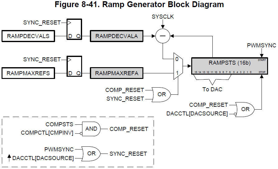
I am trying to implement a ramp generator ( saw tooth type) using the DAC sub-module for peak current mode DC converter slope compensation, based on the info discussed in this app note:
http://www.ti.com/lit/an/sprabe7a/sprabe7a.pdf
I have written the code, but I need to test it. Can anyone tell me how to view the ramp on the scope or on the emulator( I know there is a feature for graphing data while in debug mode).
I need to make sure that the ramp starts as soon as PWM1 goes high and keep decreasing by the slope value I set till it gets to zero by the end of each PWM cycle.
Thank you!
farid,
The SHADOW registers are designed specifically to buffer mid-cycle updates of values. The SHADOW registers are ignored by the ramp generator until a PWMSYNC event is received, which prompts the hardware to copy the SHADOW values into the ACTIVE registers where they can take effect.
-Tommy
farid,
Correct, the COMP1OUT output will only change when V+ and V- cross each other.
I have not done this myself, but you should be able to read back the values of RAMPSTS and DACVAL using the CPU while the ramp generator is decrementing. So if you want to prove the ramp generator behavior, you can set an EPWM CMP interrupt a few cycles before the end of a cycle and then use a CPU loop in the ISR to store a buffer of TBCTR vs RAMPSTS vs DACVAL values so that you can trace the sequence of events offline.
To calculate the RAMPDECVAL, you would probably want to determine the desired slope in mV/us terms first. The 10b DAC would give you an LSB step of VDDA/2^10, so about 3.2mV per step. The ramp generator decrements at SYSCLK so you would have one decrement operation about every 11.1ns with a 90MHz SYSCLK.
-Tommy
Hi,
Just to double check! I read at this app note: "Digital Peak Current Mode Control With Slope Compensation Using the TMS320F2803x" that Each step of the discrete ramp requires three instructions to complete.Is this still the case for TMS320F28069. You mentioned above that each decrement takes one system clock cycle.
Is there any example code I can refer to for Ramp slope compensation?
Thanks,
Farid
Farid,
I think the reason for the three instruction cycles is because they are using the CLA to generate the slope rather than the tightly coupled ramp generator hardware of the comparator:
The Biricha code uses the Control Law Accelerator (CLA) of the TMS320F2803x to implement the slope compensation. The CLA is an integrated floating-point core that allows high speed, real-time control algorithms to be executed in parallel with the main CPU.
It sounds reasonable for the CLA to take three cycles to calculate the next DAC code and write the value to the DACVAL register.
There is a PCMC implementation example for the HVPSFB kit, but it can be a little difficult to follow:
\controlSUITE\development_kits\HVPSFB_v1.1\HVPSFB_PCMC\
-Tommy