This thread has been locked.
If you have a related question, please click the "Ask a related question" button in the top right corner. The newly created question will be automatically linked to this question.
Hi,
I am trying to run the example <C2000WAREINSTALLDIR>\device_support\f2837xd\examples\cpu1\hrpwm_deadband_sfo_v8 in CPU2. I am running GPIO initialization required for ePWM and allocating the ePWMs required to CPU2 in CPU1 as below
EALLOW;
CpuSysRegs.PCLKCR0.bit.TBCLKSYNC = 0;
CpuSysRegs.PCLKCR2.bit.EPWM1 = 0;
CpuSysRegs.PCLKCR2.bit.EPWM2 = 0;
/* Assign used PWM modules to CPU2 */
DevCfgRegs.CPUSEL0.bit.EPWM1 = 1;
DevCfgRegs.CPUSEL0.bit.EPWM2 = 1;
EDIS;
InitEPwm1Gpio();
InitEPwm2Gpio();
Then I perform the rest of ePWM1 and ePWM2 configuration, setting up of ISR and modification of HR period, phase inside ISR in CPU2 after enabling the clock as below
EALLOW;
CpuSysRegs.PCLKCR0.bit.TBCLKSYNC = 0;
CpuSysRegs.PCLKCR2.bit.EPWM1 = 1;
CpuSysRegs.PCLKCR2.bit.EPWM2 = 1;
EDIS;
//
// Init HRPWM1/HRPWM2
//
HRPWM1_Config(360);
HRPWM2_Config(360);
EALLOW;
CpuSysRegs.PCLKCR0.bit.TBCLKSYNC = 1; // Resync PWM timebase clock
(*ePWM[PWM1]).GLDCTL2.bit.OSHTLD = 1; // This should also write to
// GLDCTL2 of PWM2
EDIS;
//
// Configure ePWM1 to generate interrupts on period match
//
(*ePWM[PWM1]).ETSEL.bit.INTSEL = 1; // Interrupt on counter zero match
(*ePWM[PWM1]).ETSEL.bit.INTEN = 1; // Enable peripheral interrupt
(*ePWM[PWM1]).ETPS.bit.INTPRD = 1; // Generate interrupt on every event
PieCtrlRegs.PIEIER3.bit.INTx1 = 1; // Enable ePWM1 interrupt in PIE
IER |= 0x0004; // Enable core INT #3
EINT;
But when I check all the registers of ePWM1 and ePWM2 I see the values are set correctly except for HRCNFG register. I am not sure why this is happening. This issue is not present in CPU1 as I am able to run the example code properly in CPU1. And this issue affects only HRCNFG register and does not impact any other register settings.
I have attached screenshots from CCS with break point set to the particular instruction which will update HRCNFG register value for ePWM1, after executing the instruction by stepping over the code I still cannot observe the value in debug window but if I step through the next instruction which will set HRPE value in HRPCTL register it is updated properly.
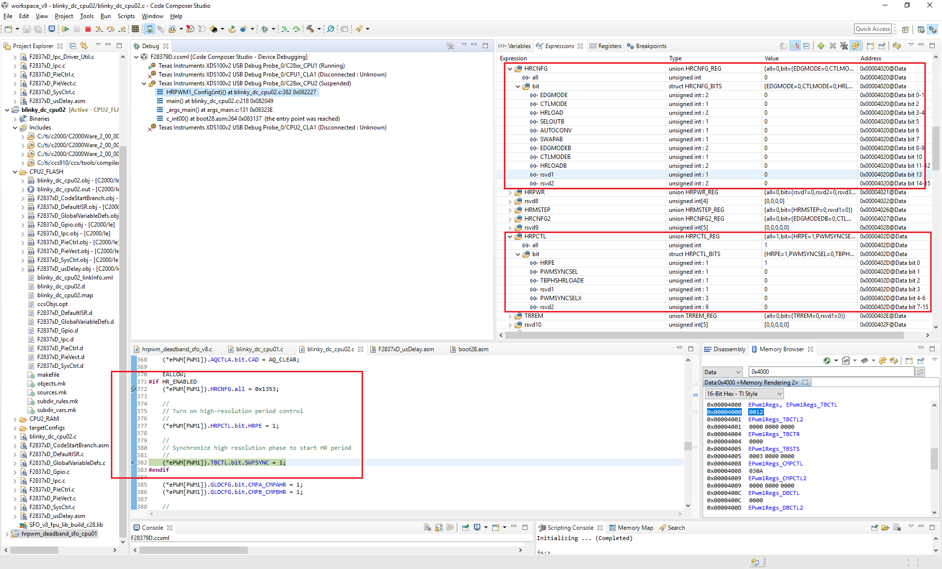
I have also ensured that the ePWM1 and ePWM2 are allocated properly to CPU2 and clock is enabled for both ePWM1 and ePWM2.
I have also attached the source code which I have used for both CPU1 and CPU2.
CPU1
//########################################################################### // // FILE: blinky_dc_hrpwm_init_cpu01.c // // TITLE: LED Blink Example along with required initialization for HRPWM to run in CPU2 for F2837xD. // //! \addtogroup dual_example_list //! <h1> Blinky </h1> //! //! Dual Core Blinky Example. This example demonstrates how to implement //! and run a standalone application on both cores. //! // //########################################################################### // $TI Release: F2837xD Support Library v3.06.00.00 $ // $Release Date: Mon May 27 06:48:24 CDT 2019 $ // $Copyright: // Copyright (C) 2013-2019 Texas Instruments Incorporated - http://www.ti.com/ // // Redistribution and use in source and binary forms, with or without // modification, are permitted provided that the following conditions // are met: // // Redistributions of source code must retain the above copyright // notice, this list of conditions and the following disclaimer. // // Redistributions in binary form must reproduce the above copyright // notice, this list of conditions and the following disclaimer in the // documentation and/or other materials provided with the // distribution. // // Neither the name of Texas Instruments Incorporated nor the names of // its contributors may be used to endorse or promote products derived // from this software without specific prior written permission. // // THIS SOFTWARE IS PROVIDED BY THE COPYRIGHT HOLDERS AND CONTRIBUTORS // "AS IS" AND ANY EXPRESS OR IMPLIED WARRANTIES, INCLUDING, BUT NOT // LIMITED TO, THE IMPLIED WARRANTIES OF MERCHANTABILITY AND FITNESS FOR // A PARTICULAR PURPOSE ARE DISCLAIMED. IN NO EVENT SHALL THE COPYRIGHT // OWNER OR CONTRIBUTORS BE LIABLE FOR ANY DIRECT, INDIRECT, INCIDENTAL, // SPECIAL, EXEMPLARY, OR CONSEQUENTIAL DAMAGES (INCLUDING, BUT NOT // LIMITED TO, PROCUREMENT OF SUBSTITUTE GOODS OR SERVICES; LOSS OF USE, // DATA, OR PROFITS; OR BUSINESS INTERRUPTION) HOWEVER CAUSED AND ON ANY // THEORY OF LIABILITY, WHETHER IN CONTRACT, STRICT LIABILITY, OR TORT // (INCLUDING NEGLIGENCE OR OTHERWISE) ARISING IN ANY WAY OUT OF THE USE // OF THIS SOFTWARE, EVEN IF ADVISED OF THE POSSIBILITY OF SUCH DAMAGE. // $ //########################################################################### // // Included Files // #include "F28x_Project.h" #include "F2837xD_Ipc_drivers.h" // // Main // void main(void) { // // Step 1. Initialize System Control: // PLL, WatchDog, enable Peripheral Clocks // This example function is found in the F2837xD_SysCtrl.c file. // InitSysCtrl(); EALLOW; ClkCfgRegs.SYSCLKDIVSEL.bit.PLLSYSCLKDIV = 1; EDIS; #ifdef _STANDALONE #ifdef _FLASH // // Send boot command to allow the CPU2 application to begin execution // IPCBootCPU2(C1C2_BROM_BOOTMODE_BOOT_FROM_FLASH); #else // // Send boot command to allow the CPU2 application to begin execution // IPCBootCPU2(C1C2_BROM_BOOTMODE_BOOT_FROM_RAM); #endif #endif // // Call Flash Initialization to setup flash waitstates // This function must reside in RAM // #ifdef _FLASH InitFlash(); #endif // // Step 2. Initialize GPIO: // This example function is found in the F2837xD_Gpio.c file and // illustrates how to set the GPIO to it's default state. // InitGpio(); // Skipped for this example EALLOW; GpioCtrlRegs.GPADIR.bit.GPIO31 = 1; GPIO_SetupPinOptions(34, GPIO_OUTPUT, GPIO_PUSHPULL); GPIO_SetupPinMux(34, GPIO_MUX_CPU2, 0); // // TODO Add code to allow configuration of GPADIR from CPU02 using IPC // EDIS; EALLOW; CpuSysRegs.PCLKCR0.bit.TBCLKSYNC = 0; CpuSysRegs.PCLKCR2.bit.EPWM1 = 0; CpuSysRegs.PCLKCR2.bit.EPWM2 = 0; /* Assign used PWM modules to CPU2 */ DevCfgRegs.CPUSEL0.bit.EPWM1 = 1; DevCfgRegs.CPUSEL0.bit.EPWM2 = 1; EDIS; InitEPwm1Gpio(); InitEPwm2Gpio(); GpioDataRegs.GPADAT.bit.GPIO31 = 1;// turn off LED // // Step 3. Clear all interrupts and initialize PIE vector table: // Disable CPU interrupts // DINT; // // Initialize the PIE control registers to their default state. // The default state is all PIE interrupts disabled and flags // are cleared. // This function is found in the F2837xD_PieCtrl.c file. // InitPieCtrl(); // // Disable CPU interrupts and clear all CPU interrupt flags: // IER = 0x0000; IFR = 0x0000; // // Initialize the PIE vector table with pointers to the shell Interrupt // Service Routines (ISR). // This will populate the entire table, even if the interrupt // is not used in this example. This is useful for debug purposes. // The shell ISR routines are found in F2837xD_DefaultIsr.c. // This function is found in F2837xD_PieVect.c. // InitPieVectTable(); // // Enable global Interrupts and higher priority real-time debug events: // EINT; // Enable Global interrupt INTM ERTM; // Enable Global realtime interrupt DBGM // // Step 6. IDLE loop. Just sit and loop forever (optional): // for(;;) { // // Turn on LED // GpioDataRegs.GPADAT.bit.GPIO31 = 0; // // Delay for a bit. // DELAY_US(1000 * 500); // // Turn off LED // GpioDataRegs.GPADAT.bit.GPIO31 = 1; // // Delay for a bit. // DELAY_US(1000 * 500); } } // // End of file //
CPU2
//########################################################################### // // FILE: hrpwm_deadband_sfo_cpu02.c // // TITLE: LED Blink and HRPWM with deadband Example for F2837xD. // // Dual Core Blinky Example. This example demonstrates how to run a // implement a standalone application on both cores. // //########################################################################### // $TI Release: F2837xD Support Library v3.06.00.00 $ // $Release Date: Mon May 27 06:48:24 CDT 2019 $ // $Copyright: // Copyright (C) 2013-2019 Texas Instruments Incorporated - http://www.ti.com/ // // Redistribution and use in source and binary forms, with or without // modification, are permitted provided that the following conditions // are met: // // Redistributions of source code must retain the above copyright // notice, this list of conditions and the following disclaimer. // // Redistributions in binary form must reproduce the above copyright // notice, this list of conditions and the following disclaimer in the // documentation and/or other materials provided with the // distribution. // // Neither the name of Texas Instruments Incorporated nor the names of // its contributors may be used to endorse or promote products derived // from this software without specific prior written permission. // // THIS SOFTWARE IS PROVIDED BY THE COPYRIGHT HOLDERS AND CONTRIBUTORS // "AS IS" AND ANY EXPRESS OR IMPLIED WARRANTIES, INCLUDING, BUT NOT // LIMITED TO, THE IMPLIED WARRANTIES OF MERCHANTABILITY AND FITNESS FOR // A PARTICULAR PURPOSE ARE DISCLAIMED. IN NO EVENT SHALL THE COPYRIGHT // OWNER OR CONTRIBUTORS BE LIABLE FOR ANY DIRECT, INDIRECT, INCIDENTAL, // SPECIAL, EXEMPLARY, OR CONSEQUENTIAL DAMAGES (INCLUDING, BUT NOT // LIMITED TO, PROCUREMENT OF SUBSTITUTE GOODS OR SERVICES; LOSS OF USE, // DATA, OR PROFITS; OR BUSINESS INTERRUPTION) HOWEVER CAUSED AND ON ANY // THEORY OF LIABILITY, WHETHER IN CONTRACT, STRICT LIABILITY, OR TORT // (INCLUDING NEGLIGENCE OR OTHERWISE) ARISING IN ANY WAY OUT OF THE USE // OF THIS SOFTWARE, EVEN IF ADVISED OF THE POSSIBILITY OF SUCH DAMAGE. // $ //########################################################################### // // Included Files // #include "F28x_Project.h" #include "SFO_V8.h" #ifdef _FLASH // // These are defined by the linker (see device linker command file) // extern Uint16 RamfuncsLoadStart; extern Uint16 RamfuncsLoadSize; extern Uint16 RamfuncsRunStart; #endif // // Defines // #define PWM_CH 9 // # of PWM channels + 1 #define HR_ENABLED 1 // 1 = HR behavior // 0 = non-HR behavior // // Globals // Uint16 UpdateFine, status; Uint16 temp_REM2 = 0, temp_PHS2, PhaseFine2; Uint32 CountUpdatefine = 0, CountUpdateMax = 0; Uint16 Period = 0, PeriodFine = 0, PeriodOdd = 0; Uint16 PeriodIncrement = 0, PeriodFineIncrement = 0; Uint32 InputPeriodInc = 0; Uint32 PeriodFine_temp = 0; Uint16 PWM1 = 1; Uint16 PWM2 = 2; Uint16 PeriodMax = 600, PeriodMin = 360; // // Array of pointers to EPwm register structures: // *ePWM[0] is defined as dummy value not used in the example // volatile struct EPWM_REGS *ePWM[PWM_CH] = { &EPwm1Regs, &EPwm1Regs, &EPwm2Regs, &EPwm3Regs, &EPwm4Regs, &EPwm5Regs, &EPwm6Regs, &EPwm7Regs, &EPwm8Regs}; int MEP_ScaleFactor; // // Function Prototypes // void HRPWM1_Config(int); void HRPWM2_Config(int); void FreqCtl_func(void); interrupt void PRDEQfix_ISR(void); void error(void); // // Main // void main(void) { // // Copy time critical code and Flash setup code to RAM // This includes InitFlash(), Flash API functions and any functions that are // assigned to ramfuncs section. // The RamfuncsLoadStart, RamfuncsLoadEnd, and RamfuncsRunStart // symbols are created by the linker. Refer to the device .cmd file. // #ifdef _FLASH memcpy(&RamfuncsRunStart, &RamfuncsLoadStart, (size_t)&RamfuncsLoadSize); #endif // // Step 1. Initialize System Control: // PLL, WatchDog, enable Peripheral Clocks // This example function is found in the F2837xD_SysCtrl.c file. // InitSysCtrl(); // // Call Flash Initialization to setup flash waitstates // This function must reside in RAM // #ifdef _FLASH InitFlash(); #endif // // Step 2. Initialize GPIO: // This example function is found in the F2837xD_Gpio.c file and // illustrates how to set the GPIO to it's default state. // // InitGpio(); // Skipped for this example EALLOW; // //TODO Add code to configure GPADIR through IPC // GPIO_WritePin(34, 1); // // Step 3. Clear all interrupts and initialize PIE vector table: // Disable CPU interrupts // DINT; // // Initialize the PIE control registers to their default state. // The default state is all PIE interrupts disabled and flags // are cleared. // This function is found in the F2837xD_PieCtrl.c file. // InitPieCtrl(); // // Disable CPU interrupts and clear all CPU interrupt flags: // IER = 0x0000; IFR = 0x0000; // // Initialize the PIE vector table with pointers to the shell Interrupt // Service Routines (ISR). // This will populate the entire table, even if the interrupt // is not used in this example. This is useful for debug purposes. // The shell ISR routines are found in F2837xD_DefaultIsr.c. // This function is found in F2837xD_PieVect.c. // InitPieVectTable(); // // Set address of ISR in PIE vector table // EALLOW; PieVectTable.EPWM1_INT = &PRDEQfix_ISR; EDIS; // // Enable global Interrupts and higher priority real-time debug events: // EINT; // Enable Global interrupt INTM ERTM; // Enable Global realtime interrupt DBGM // // Calling SFO() updates the HRMSTEP register with calibrated // MEP_ScaleFactor. HRMSTEP must be populated with a scale factor value // prior to enabling high resolution period control. // status = SFO_INCOMPLETE; while(status == SFO_INCOMPLETE) { // // Call until complete // status = SFO(); if (status == SFO_ERROR) { error(); } } EALLOW; CpuSysRegs.PCLKCR0.bit.TBCLKSYNC = 0; CpuSysRegs.PCLKCR2.bit.EPWM1 = 1; CpuSysRegs.PCLKCR2.bit.EPWM2 = 1; EDIS; // // Init HRPWM1/HRPWM2 // HRPWM1_Config(360); HRPWM2_Config(360); EALLOW; CpuSysRegs.PCLKCR0.bit.TBCLKSYNC = 1; // Resync PWM timebase clock (*ePWM[PWM1]).GLDCTL2.bit.OSHTLD = 1; // This should also write to // GLDCTL2 of PWM2 EDIS; // // Configure ePWM1 to generate interrupts on period match // (*ePWM[PWM1]).ETSEL.bit.INTSEL = 1; // Interrupt on counter zero match (*ePWM[PWM1]).ETSEL.bit.INTEN = 1; // Enable peripheral interrupt (*ePWM[PWM1]).ETPS.bit.INTPRD = 1; // Generate interrupt on every event PieCtrlRegs.PIEIER3.bit.INTx1 = 1; // Enable ePWM1 interrupt in PIE IER |= 0x0004; // Enable core INT #3 EINT; // Clear global interrupt mask UpdateFine = 0; // Disable continuous updates Period = 360; PeriodFine = 0x0; CountUpdateMax = 0x0FFFF; CountUpdatefine = CountUpdateMax; // // Watch window variable to modify the rate of the frequency sweep // InputPeriodInc = 6553; // // Step 6. IDLE loop. Just sit and loop forever (optional): // for(;;) { // // Turn on LED // GPIO_WritePin(34, 0); // // Delay for a bit. // DELAY_US(1000 * 250); // // Turn off LED // GPIO_WritePin(34, 1); // // Delay for a bit. // DELAY_US(1000 * 250); while(UpdateFine == 0) { if(CountUpdatefine >= CountUpdateMax) { if(Period < PeriodMax) { // // Perform sweep // PeriodIncrement = InputPeriodInc >> 16; PeriodFineIncrement = (Uint16)InputPeriodInc; Period = Period + PeriodIncrement; PeriodFine_temp = (Uint32)PeriodFine + (Uint32)PeriodFineIncrement; if(PeriodFine_temp >= 0x10000) { PeriodFine_temp = PeriodFine_temp - 0x10000; Period = Period + 1; } // // Period is odd - CMP is divide by 2 for 50% duty // if (Period % 2 == 1) { PeriodOdd = 1; } else { PeriodOdd = 0; } PeriodFine = (Uint16) PeriodFine_temp; // // Update PWM values for non-zero increment // if (InputPeriodInc != 0) { FreqCtl_func(); } } else { Period = PeriodMin; PeriodFine = 0; if (InputPeriodInc != 0) { FreqCtl_func(); } } CountUpdatefine = 0; } CountUpdatefine++; } } } // // HRPWM1_Config - ePWM1 register configuration with HRPWM // ePWM1A toggle low/high with MEP control on Rising edge // void HRPWM1_Config(PeriodConfig) { (*ePWM[PWM1]).TBCTL.bit.PRDLD = TB_SHADOW; // Set Immediate load // // PWM frequency = 1 / PeriodConfig // (*ePWM[PWM1]).TBPRD = PeriodConfig; // // Set duty 50% initially and initialize HRPWM extension // (*ePWM[PWM1]).CMPA.bit.CMPA = PeriodConfig / 2; (*ePWM[PWM1]).CMPA.bit.CMPAHR = (1 << 8); (*ePWM[PWM1]).CMPB.bit.CMPB = PeriodConfig / 2; (*ePWM[PWM1]).CMPB.bit.CMPBHR = (1 << 8); (*ePWM[PWM1]).TBPHS.all = 0; (*ePWM[PWM1]).TBCTR = 0; (*ePWM[PWM1]).TBCTL.bit.CTRMODE = TB_COUNT_UPDOWN; (*ePWM[PWM1]).TBCTL.bit.PHSEN = TB_DISABLE; // ePWM1 is the Master (*ePWM[PWM1]).TBCTL.bit.SYNCOSEL = TB_CTR_ZERO; (*ePWM[PWM1]).TBCTL.bit.HSPCLKDIV = TB_DIV1; (*ePWM[PWM1]).TBCTL.bit.CLKDIV = TB_DIV1; // // LOAD CMPA on CTR = ZERO_PRD // (*ePWM[PWM1]).CMPCTL.bit.LOADAMODE = CC_CTR_ZERO_PRD; (*ePWM[PWM1]).CMPCTL.bit.LOADBMODE = CC_CTR_ZERO_PRD; (*ePWM[PWM1]).CMPCTL.bit.SHDWAMODE = CC_SHADOW; (*ePWM[PWM1]).CMPCTL.bit.SHDWBMODE = CC_SHADOW; (*ePWM[PWM1]).AQCTLA.bit.CAU = AQ_SET; (*ePWM[PWM1]).AQCTLA.bit.CAD = AQ_CLEAR; EALLOW; #if HR_ENABLED (*ePWM[PWM1]).HRCNFG.all = 0x1353; // // Turn on high-resolution period control // (*ePWM[PWM1]).HRPCTL.bit.HRPE = 1; // // Synchronize high resolution phase to start HR period // (*ePWM[PWM1]).TBCTL.bit.SWFSYNC = 1; #endif (*ePWM[PWM1]).GLDCFG.bit.CMPA_CMPAHR = 1; (*ePWM[PWM1]).GLDCFG.bit.CMPB_CMPBHR = 1; // // Load on CTR = ZERO_PRD (2) / ZERO (1) // (*ePWM[PWM1]).GLDCTL.bit.GLDMODE = 2; // // One shot mode and global load enabled // (*ePWM[PWM1]).GLDCTL.bit.OSHTMODE = 1; (*ePWM[PWM1]).GLDCTL.bit.GLD = 1; // // Write to PWM1 GLDCTL2 will result in simultaneous write to PWM2 GLDCTL2 // (*ePWM[PWM1]).EPWMXLINK.bit.GLDCTL2LINK = PWM1 - 1; (*ePWM[PWM1]).DBCTL.bit.OUT_MODE = DB_FULL_ENABLE; (*ePWM[PWM1]).DBCTL.bit.POLSEL = DB_ACTV_HIC; (*ePWM[PWM1]).DBCTL.bit.IN_MODE = DBA_ALL; (*ePWM[PWM1]).DBCTL.bit.SHDWDBREDMODE = 1; (*ePWM[PWM1]).DBCTL.bit.SHDWDBFEDMODE = 1; (*ePWM[PWM1]).DBCTL.bit.LOADREDMODE = 0; // Load on Counter == 0 (*ePWM[PWM1]).DBCTL.bit.LOADFEDMODE = 0; // Load on Counter == 0 (*ePWM[PWM1]).DBCTL.bit.HALFCYCLE = 1; (*ePWM[PWM1]).DBRED.bit.DBRED = 4; (*ePWM[PWM1]).DBREDHR.bit.DBREDHR = 0x0; (*ePWM[PWM1]).DBFED.bit.DBFED = 4; (*ePWM[PWM1]).DBFEDHR.bit.DBFEDHR = 0x0; (*ePWM[PWM1]).HRCNFG2.bit.EDGMODEDB = HR_BEP; // DBREDHR and DBFEDHR (*ePWM[PWM1]).HRCNFG2.bit.CTLMODEDBRED = 0; // Load on ZRO (*ePWM[PWM1]).HRCNFG2.bit.CTLMODEDBFED = 0; // Load on ZRO (*ePWM[PWM1]).DBREDHR.bit.DBREDHR = (0 << 9); EDIS; } // // HRPWM2_Config - ePWM2 register configuration with HRPWM // ePWM2A toggle low/high with MEP control on Rising edge // void HRPWM2_Config(PeriodConfig) { (*ePWM[PWM2]).TBCTL.bit.PRDLD = TB_SHADOW; // Set Immediate load // // PWM frequency = 1 / PeriodConfig // (*ePWM[PWM2]).TBPRD = PeriodConfig; // // Set duty 50% initially and initialize HRPWM extension // (*ePWM[PWM2]).CMPA.bit.CMPA = PeriodConfig / 2; (*ePWM[PWM2]).CMPA.bit.CMPAHR = (1 << 8); (*ePWM[PWM2]).CMPB.bit.CMPB = PeriodConfig / 2; (*ePWM[PWM2]).CMPB.bit.CMPBHR = (1 << 8); (*ePWM[PWM2]).TBPHS.all = 0; (*ePWM[PWM2]).TBCTR = 0; (*ePWM[PWM2]).TBCTL.bit.CTRMODE = TB_COUNT_UPDOWN; (*ePWM[PWM2]).TBCTL.bit.PHSEN = TB_DISABLE; // ePWM1 is the Master (*ePWM[PWM2]).TBCTL.bit.SYNCOSEL = TB_SYNC_IN; (*ePWM[PWM2]).TBCTL.bit.HSPCLKDIV = TB_DIV1; (*ePWM[PWM2]).TBCTL.bit.CLKDIV = TB_DIV1; // // LOAD CMPA on CTR = 0 // (*ePWM[PWM2]).CMPCTL.bit.LOADAMODE = CC_CTR_ZERO_PRD; (*ePWM[PWM2]).CMPCTL.bit.LOADBMODE = CC_CTR_ZERO_PRD; (*ePWM[PWM2]).CMPCTL.bit.SHDWAMODE = CC_SHADOW; (*ePWM[PWM2]).CMPCTL.bit.SHDWBMODE = CC_SHADOW; (*ePWM[PWM2]).AQCTLA.bit.CAU = AQ_SET; (*ePWM[PWM2]).AQCTLA.bit.CAD = AQ_CLEAR; EALLOW; #if HR_ENABLED (*ePWM[PWM2]).HRCNFG.all = 0x1353; // // Turn on high-resolution period control // (*ePWM[PWM2]).HRPCTL.bit.HRPE = 1; // // Synchronize high resolution phase to start HR period // (*ePWM[PWM2]).TBCTL.bit.SWFSYNC = 1; #endif (*ePWM[PWM2]).TBCTL.bit.PHSDIR = 1; // Count up after SYNC event (*ePWM[PWM2]).TBPHS.bit.TBPHS = 180; (*ePWM[PWM2]).GLDCFG.bit.CMPA_CMPAHR = 1; (*ePWM[PWM2]).GLDCFG.bit.CMPB_CMPBHR = 1; // // Load on CTR = ZERO_PRD (2) / ZERO (1) // (*ePWM[PWM2]).GLDCTL.bit.GLDMODE = 2; // // One shot mode and global load enabled // (*ePWM[PWM2]).GLDCTL.bit.OSHTMODE = 1; (*ePWM[PWM2]).GLDCTL.bit.GLD = 1; // // Write to PWM1 GLDCTL2 will result in simultaneous write to PWM2 GLDCTL2 // (*ePWM[PWM2]).EPWMXLINK.bit.GLDCTL2LINK = PWM1 - 1; (*ePWM[PWM2]).DBCTL.bit.OUT_MODE = DB_FULL_ENABLE; (*ePWM[PWM2]).DBCTL.bit.POLSEL = DB_ACTV_HIC; (*ePWM[PWM2]).DBCTL.bit.IN_MODE = DBA_ALL; (*ePWM[PWM2]).DBCTL.bit.SHDWDBREDMODE = 1; (*ePWM[PWM2]).DBCTL.bit.SHDWDBFEDMODE = 1; (*ePWM[PWM2]).DBCTL.bit.LOADREDMODE = 0; // Load on Counter == 0 (*ePWM[PWM2]).DBCTL.bit.LOADFEDMODE = 0; // Load on Counter == 0 (*ePWM[PWM2]).DBCTL.bit.HALFCYCLE = 1; (*ePWM[PWM2]).DBRED.bit.DBRED = 4; (*ePWM[PWM2]).DBREDHR.bit.DBREDHR = 0x0; (*ePWM[PWM2]).DBFED.bit.DBFED = 4; (*ePWM[PWM2]).DBFEDHR.bit.DBFEDHR = 0x0; (*ePWM[PWM2]).HRCNFG2.bit.EDGMODEDB = HR_BEP; // DBREDHR and DBFEDHR (*ePWM[PWM2]).HRCNFG2.bit.CTLMODEDBRED = 0; // Load on ZRO (*ePWM[PWM2]).HRCNFG2.bit.CTLMODEDBFED = 0; // Load on ZRO (*ePWM[PWM2]).DBREDHR.bit.DBREDHR = (0 << 9); EDIS; } // // FreqCtl_func - Frequency modulation & phase sync function // This function is called only if frequency sweep is enabled // void FreqCtl_func(void) { if (PeriodOdd) { // // Add 0.5 if period is odd // (*ePWM[PWM1]).CMPA.bit.CMPAHR = (PeriodFine >> 1) + 0x7FFF; (*ePWM[PWM2]).CMPA.bit.CMPAHR = (PeriodFine >> 1) + 0x7FFF; (*ePWM[PWM1]).CMPB.bit.CMPBHR = (PeriodFine >> 1) + 0x7FFF; (*ePWM[PWM2]).CMPB.bit.CMPBHR = (PeriodFine >> 1) + 0x7FFF; } else { (*ePWM[PWM1]).CMPA.bit.CMPAHR = PeriodFine >> 1; (*ePWM[PWM2]).CMPA.bit.CMPAHR = PeriodFine >> 1; (*ePWM[PWM1]).CMPB.bit.CMPBHR = PeriodFine >> 1; (*ePWM[PWM2]).CMPB.bit.CMPBHR = PeriodFine >> 1; } (*ePWM[PWM1]).CMPA.bit.CMPA = (Period >> 1) + 1; (*ePWM[PWM2]).CMPA.bit.CMPA = (Period >> 1) + 1; (*ePWM[PWM1]).CMPB.bit.CMPB = (Period >> 1) + 1; (*ePWM[PWM2]).CMPB.bit.CMPB = (Period >> 1) + 1; temp_PHS2 = (Period >> 1); switch(PeriodOdd) { case 1: // // Accounting for divide by 2 = 0.5 // PhaseFine2 = 0xFF - (PeriodFine >> 9) - 0x7F; break; default: PhaseFine2 = 0xFF - (PeriodFine >> 9); break; } // // No fractional phase shift to account for // temp_REM2 = (Uint16) 0x100 + PhaseFine2; UpdateFine = 1; } // // PRDEQfix_ISR - ISR for Translator remainder calculations // interrupt void PRDEQfix_ISR(void) { EALLOW; if (UpdateFine == 1) { // // This should also write to GLDCTL2 of PWM2, PWM3 and PWM4 // (*ePWM[PWM1]).GLDCTL2.bit.OSHTLD = 1; // // TBCTR phase load on SYNC (required for updown count HR control // (*ePWM[PWM2]).TBCTL.bit.PHSEN = TB_ENABLE; // // Coarse phase offset relative to ePWM1 // (*ePWM[PWM2]).TBPHS.bit.TBPHS = temp_PHS2; (*ePWM[PWM2]).TRREM.bit.TRREM = temp_REM2; (*ePWM[PWM2]).TBPRDHR = PeriodFine; (*ePWM[PWM2]).TBPRD = Period; (*ePWM[PWM1]).TBPRDHR = PeriodFine; (*ePWM[PWM1]).TBPRD = Period; (*ePWM[PWM1]).TRREM.bit.TRREM = 0x100; UpdateFine = 0; } else { (*ePWM[PWM2]).TBCTL.bit.PHSEN = TB_DISABLE; } // // Re-initialize for next PWM interrupt // PieCtrlRegs.PIEACK.all = PIEACK_GROUP3; // Acknowledge PIE interrupt (*ePWM[PWM1]).ETCLR.bit.INT = 1; // Clear interrupt bit EDIS; } void error (void) { ESTOP0; // Stop here and handle error } // // End of file //
Please let me know how to solve this problem.
Thanks,
Aditya
Hi Nima,
Two questions
1) Can you point me to the doc which says SFO is available only in CPU1? Does this mean we cannot consider MEP_ScaleFactor in any calculations for HRPWM in CPU2 or its just the SFO() function call will not work and this has to be done in CPU1?
2) Also HRCNFG register is just not only about SFO right? for HRCNFG = 0x1353 we will have following values
EDGEMODE = 3
CTLMODE=0
HRLOAD = 2
SELOUTB = 0
AUTOCONV = 1 (which will enable SFO)
SWAPB = 0
EDGEMODEB = 3
CTLMODEB = 0
HRLOADB = 1
which will have impact on how the HRPWM waveform needs to respond right? But these values are not being set. In TRM only SyncSocRegs and EPwmXbarRegs are indicated to be available in CPU1. So then how to proceed with HRPWM configuration for this?
Thanks,
Aditya
In this device, the HR configuration part of the ePWM modules only exists on ePWM1. Also SFO only runs on CPU1. Therefore ePWM1 must be allocated to CPU1 and SFO must run on CPU1.
Hi Nima,
Thanks, for the reply.
I am assuming this statement "In this device, the HR configuration part of the ePWM modules only exists on ePWM1." means that HRCNFG for ePWM works only for CPU1 and does not work on CPU2 for all ePWMs. Please correct me if I am wrong.
Is this true for all multicore devices like F28388D for instance?
Can you update the TRM for the devices with this additional information. I do not see this in our current version of TRM.
Thanks,
Aditya
For F28388D device, eventhough CPU and EWPM1 still do the calibration for HRPWM, each EPWM module clocks the own HRPWM, and use the same copy of HRMSTEP calculated by the SFO. This allows HRPWM to function correctly with CPU2.
Refer to the diagram in the TRM:
HRPWM and HRCAL Source Clock