This thread has been locked.

If you have a related question, please click the "Ask a related question" button in the top right corner. The newly created question will be automatically linked to this question.

TMS320F2812: XINTF on F2812 to EMIF on 28379D

Part Number: TMS320F2812
Other Parts Discussed in Thread: PROFIBUS

Hi everybody,

I'm doing a software migration from a F2812 MUC to a F28379D. 

Currently, I'm working on the EMIF part, to communicate with an asynchronous RAM (8 bits).
Below the wiring :

Is it correct?

In the F2812 software, there's not configuration file for the XINTF. I saw in this thread https://e2e.ti.com/support/microcontrollers/c2000/f/171/t/282734?failure-on-Xintf-initialization that 

On F2812 device, the XINTF is active by default out of reset.  Timings are all configured for maximum (meaning, slowest) since this is safe.

So normally, all the timing register are set like this :

So normally, for a write cycle, Txzcs0 = XWRLEAD + XWRACTIVE + XWRTRAIL = 347ns.
With the oscilloscope, I find around 360ns, so it's ok

Now I set all the registers for the F28379D to have the same timing than F2812 : 

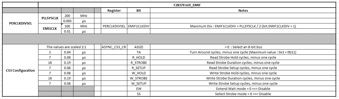
So normally, for a write cycle, Tcs3 = W_HOLD+ W_STROBE+ W_SETUP= 350ns.
With the oscilloscope, I find around 700ns. Why?

Thanks for your reply.

  • electrocc,

    Is it possible that you are observing the time for two back-to-back accesses?  The C28x is 16b-word addressible so each access will generate two 8b operations.

    This behavior is briefly covered in the EMIF appnote.

    -Tommy

  • Hi Tommy,

    Yes I think this is what's happens. So how can I proceed to write only one 8b operations?

    For example,  I want to write 8 bits data to the address 0x3FFE, and read datas (8 bits) to the adresses 0x3FFF?

    Regards

  • Hi,

    If I've understood the appnote, if I want to send data "0xA0" for example, first write is "0xA0" and second write is "0x00"?
    How can I proceed to send only one word "0xA0"?

    Because if the data viewed by the external memory is the 2nd write, it's not correct (0x00 instead of 0xFE)

    Regards,

  • electrocc,

    C28x address will always represent 16-bits of data so you will always write in 16-bit increments.

    Each Write operation shown in the table represents an atomic operation that acts upon different addresses as seen by the external memory.

    -Tommy

  • Hi,

    TMS320F2812 belongs also to the C28x familly? So the behavior is the same between F2812 and F28379D?

  • Yes, any device with the C28x processor will inherit its instruction set architecture.

  • Hi,

    Thank you for your answer.
    It's still doesn't work.


    I've checked my hardware, it's ok. My external memory is a DPRAM, not an SRAM. Is this the cause of the problem?
    The same software worked with a F2812. Does the 2812 can work with a DPRAM and not the 28379D?

    The software to test is very simple, I send a data on a specific address on the memory, this one must return the same value (on a different address) to the MCU (below datasheet of the memory) :

    They are sent in a ping-pong protocol, i.e. the application sends a telegram, including at least control information, to the module and waits for a telegram in return before it sends the next telegram.The return telegram always includes at least status information.

    Regards

  • electrocc,

    The underlying memory implementation is not important as long as it conforms to the standard SRAM interface.

    Have you checked your EMIF settings against the configuration spreadsheet tool?  This will help to roughly check the registers.

    If there are still problems, we will need to know which specific signal(s) are misbehaving (and in what manner) in order to help you debug further.  This will ultimately require a methodical comparison of the observed EMIF signal activity against the F28379D and memory datasheets.

    -Tommy

  • Hi Tommy,

    The external memory I use is in reality a Profibus module (by Anybus), which have a DPRAM (my old software based on the 2812 worked with this module).

    Below a quick explanation of the communication between the MCU and the DPRAM :

    After initialization steps (see datasheet hms-hmsi-168-106.pdf page 10, step 1 "Connect Module" to step 3 "Initial Handshake"), there is a step called "Send and received telegrams" ; in this step, when I send a message (0xA0) to the DPRAM on the specific register (Control Register at address 0x3FFE (datasheet page 16-17)), this one returns a message(0xA0) to the MCU on another register (Status Register at address 0x3FFF (datasheet page 16-17))

    This is to ensure that communication between MCU and DPRAM  works properly.

    My software does only these steps : initialization steps and communication test. I put a asm ("      ESTOP0"); in my code after writing in the RAM :

    • For the F2812, data on 0x3FFE address (Control Register) (i used XINTF Zone 0) is 0xA0 ; data on 0x3FFF adress (Status Register) is 0xA0 (answer from the DPRAM)

    • For the F28379D, data on 0x303FFE address (Control Register) (i used CS3 ASYNC) is 0xA0 ; data on 0x303FFF address (Status Register) is 0x00 (no answer from the DPRAM)

    Below my EMIF settings :

    extern void Emif1Initialize(void);
    
    //---------------------------------------------
    /// \fn void Init_EMIF(void)
    ///
    /// \brief Control registers for EMIF.
    /// \param None.
    /// \return None.
    
    void Init_EMIF(void)
    {
        // ---------- Declaration ----------
    
        Emif1Initialize();
        //
        //Configure to run EMIF1 on half Rate (EMIF1CLK = CPU1SYSCLK / 2)
        //
        EALLOW;
        ClkCfgRegs.PERCLKDIVSEL.bit.EMIF1CLKDIV = 0x1;
        EDIS;
    
        EALLOW;
        //
        // Grab EMIF1 For CPU1
        //
        Emif1ConfigRegs.EMIF1MSEL.all = 0x93A5CE71;
    
        //
        //Disable Access Protection (CPU_FETCH/CPU_WR/DMA_WR)
        //
        Emif1ConfigRegs.EMIF1ACCPROT0.all = 0x0;
    
        //
        // Commit the configuration related to protection. Till this bit remains set
        // content of EMIF1ACCPROT0 register can't be changed.
        //
        Emif1ConfigRegs.EMIF1COMMIT.all = 0x1;
    
        //
        // Lock the configuration so that EMIF1COMMIT register can't be
        // changed any more.
        //
        Emif1ConfigRegs.EMIF1LOCK.all = 0x1;
    
        //
        //Configure the access timing for CS3 space
        //
    
        Emif1Regs.ASYNC_CS3_CR.bit.ASIZE = 0;       // Asynchronous Device Bus Width. ASIZE = 0 selects an 8-bit bus
        Emif1Regs.ASYNC_CS3_CR.bit.TA = 3;          // Number of EMxCLK cycles between the end of one asynchronous memory access and the start of another asynchronous memory access, minus one cycle
        Emif1Regs.ASYNC_CS3_CR.bit.R_HOLD = 7;      // Read hold widths.
        Emif1Regs.ASYNC_CS3_CR.bit.R_STROBE = 18;   // Read Strobe Duration cycles
        Emif1Regs.ASYNC_CS3_CR.bit.R_SETUP = 7;     // Read Strobe Setup cycles
        Emif1Regs.ASYNC_CS3_CR.bit.W_HOLD = 7;      // Write hold widths.
        Emif1Regs.ASYNC_CS3_CR.bit.W_STROBE = 18;   // Write Strobe Duration cycles
        Emif1Regs.ASYNC_CS3_CR.bit.W_SETUP = 7;     // Write Strobe Setup cycles
        Emif1Regs.ASYNC_CS3_CR.bit.EW = 0;          // Extended Wait Mode enable. EW = 0 disables extended wait mode
        Emif1Regs.ASYNC_CS3_CR.bit.SS = 0;          // Select Strobe mode. SS = 0 selects Normal Mode
    
        Emif1Regs.RCSR.bit.BE = 0;                  // EMIF endian mode = 0: Little Endian
        Emif1Regs.RCSR.bit.FR = 0;                  // EMIF operating rate = 1: Full Rate
    
        EDIS;
    }

    I can share with you observed EMIF signal activity at the same time (immediately after writing in the RAM).

    I share with you also the configuration spreadsheet tool with CS3 configuration.C2000-EMIF_ConfigurationTool.xlsx

    Regards,

    hms-hmsi-168-106.pdf

  • electrocc,

    Yes, please investigate the signal activity to make sure that they match what you expect.

    Also, please continue to keep in mind that the C28x is 16b-word addressable.  The C28x 16b 0x303FFF address will not map to the same location as the external 8b 0x3FFF offset.

    -Tommy

  • Hi Tommy,

    So it could explain the issue? If I write on the address 0X303FFE, it doesn't match with the address 0x3FFE in the external memory?
    But why does it works with the F2812?

    Regards

  • electrocc,

    Were you able to investigate your EMIF signal activity?  I would prefer not to speculate about differences in the systems until you are able to positively identify the root cause of the failure in your F28379D system.

    -Tommy

  • Hi Tommy,

    I thought EMIF curves I had on my laptop were getted during a writing operation, but I'm not sure because the /WE signal is always in high state (maybe it is during a first read of the external memory).

    I have no access to an oscilloscope until Tuesday, but if I get EMIF signal during first write, how it could help me?
    What signals do I have to analyze?

    Regards

  • Tlee,

    I'm agree that C28x is 16b-word addressable. But why do you say external memory is 8b-(byte) addressable?

    So I have to divide all my addresses by 2?
    One address on C28x correspond to 2 addresses in external memory? (example : address 0x0030 0000 on C28x correspond to addresses 0x0000 and 0x0001 in external memory?)

    Following what you said, if I want to write, for example, to the Control register (address 0x3FFE in the memory), I have to write on address 0x0030 1FFF on C28x?

    If it works like that, for example, how can I have access to only Status Register (address 0x3FFF in the memory) on address 0x0030 1FFF, and not to the Control Register (address 0x3FFE in the memory)?

    Regards

  • electrocc said:
    I'm agree that C28x is 16b-word addressable. But why do you say external memory is 8b-(byte) addressable?

    From what I understand, the external device has an 8b data bus....hence 8b addressable.

    electrocc said:
    ISo I have to divide all my addresses by 2?
    One address on C28x correspond to 2 addresses in external memory? (example : address 0x0030 0000 on C28x correspond to addresses 0x0000 and 0x0001 in external memory?)

    Following what you said, if I want to write, for example, to the Control register (address 0x3FFE in the memory), I have to write on address 0x0030 1FFF on C28x?

    Yes, each 16b access will produce two 8b operations.

    The purpose of observing the EMIF signals is to confirm the address bus translation from the C28x access to the external device. I am not comfortable with treating this theory as the root cause of your issue without confirmation. You can certainly experiment with different addresses to see if they line up with expectations.

    electrocc said:
    If it works like that, for example, how can I have access to only Status Register (address 0x3FFF in the memory) on address 0x0030 1FFF, and not to the Control Register (address 0x3FFE in the memory)?

    You would probably be able to do this by configuring the EMIF to operate in 16b mode and only using the 8 least significant bits of each C28x word.

  • Hi Tommy,

    I want to write 8 datas to the external memory, so obtain datas like below :

    (1)

    - External memory offset 0x3B00 : Data = 0x01
    - External memory offset 0x3B01 : Data = 0x01
    - External memory offset 0x3B02 : Data = 0x01
    - External memory offset 0x3B03 : Data = 0x00
    - External memory offset 0x3B04 : Data = 0x41
    - External memory offset 0x3B05 : Data = 0x00
    - External memory offset 0x3B06 : Data = 0x01
    - External memory offset 0x3B07 : Data = 0x00

    Following what you've said, each 16b access produce two 8b operations.

    I use this (part of) code :

    #define ABCC_PARALLEL_BASE_ADDRESS        0x300000
    #define iDpramOffset                      0x1D80
    
    UINT16      iBytes = 8;
    UINT8*      pabDpram;
    
        pabDpram = (UINT8*)( ABCC_PARALLEL_BASE_ADDRESS + iDpramOffset );
    
       for( iBytes = 0; iBytes < iLength; iBytes++ )
        {
            *pabDpram++ = (*pbSource++);
        }

    I've the issue I've expected : 

    The external memory will see :

    - External memory offset 0x3B00 (address 0x301D80 on C28x) : Data = 0x01
    - External memory offset 0x3B01 (address 0x301D80 on C28x) : Data = 0x00

    - External memory offset 0x3B02 (address 0x301D81 on C28x) : Data = 0x01
    - External memory offset 0x3B03 (address 0x301D81 on C28x) : Data = 0x00

    - External memory offset 0x3B04 (address 0x301D82 on C28x) : Data = 0x01
    - External memory offset 0x3B05 (address 0x301D82 on C28x) : Data = 0x00

    - External memory offset 0x3B06 (address 0x301D83 on C28x) : Data = 0x00
    - External memory offset 0x3B07 (address 0x301D83 on C28x) : Data = 0x00

    - External memory offset 0x3B08 (address 0x301D84 on C28x) : Data = 0x41
    - External memory offset 0x3B09 (address 0x301D84 on C28x) : Data = 0x00

    - External memory offset 0x3B0A (address 0x301D85 on C28x) : Data = 0x00
    - External memory offset 0x3B0B (address 0x301D85 on C28x) : Data = 0x00

    - External memory offset 0x3B0C (address 0x301D86 on C28x) : Data = 0x01
    - External memory offset 0x3B0D (address 0x301D86 on C28x) : Data = 0x00

    - External memory offset 0x3B0E (address 0x301D87 on C28x) : Data = 0x00
    - External memory offset 0x3B0F (address 0x301D87 on C28x) : Data = 0x00

    How can I have the same result than above (1)?

    I need to use byte Intrinsic?

    Why there 're differences between F2812 and F28379D? Both of them belongs to C28x?!

    Regards

  • electrocc,

    As I had suggested in my prior post, I think your primary course of action should now be to configure the EMIF to operate in 16b mode:

    tlee said:
    You would probably be able to do this by configuring the EMIF to operate in 16b mode and only using the 8 least significant bits of each C28x word.

    Keep in mind that your original line of questioning led us to assume that you were using the EMIF with a generic 8-bit external RAM for data storage. With the revelation that the EMIF is being used to interface with an external controller, the debug approach and solution should be appropriately adapted.

    I suspect that the F2812 XINTF is operating in 16b mode with only the lower 8b used per C28x address.

    -Tommy

  • Tommy,

    I've changed the software and wiring to operate in 16b mode.

    Emif1Regs.ASYNC_CS3_CR.bit.ASIZE = 1;       // Asynchronous Device Bus Width. ASIZE = 1 selects an 16-bit bus

    I'm a little bit confused.

    Previously you told me :

    The C28x 16b 0x303FFF address will not map to the same location as the external 8b 0x3FFF offset.

    Yes, each 16b access will produce two 8b operations.

    But now, I'm in 16-bit mode ; so normally :

    • if I send data on 0x303FFE address, it will map to 0x3FFE offset?
    • Received data will be correct because only the lower 8b (connected to my memory D0-->D7) are used?


    I've observing the EMIF signals, and everything seemed to be ok.

    Regards

  • electrocc said:
    I'm a little bit confused.

    Previously you told me :

    The C28x 16b 0x303FFF address will not map to the same location as the external 8b 0x3FFF offset.

    Yes, each 16b access will produce two 8b operations.

    But now, I'm in 16-bit mode ; so normally :

    • if I send data on 0x303FFE address, it will map to 0x3FFE offset?
    • Received data will be correct because only the lower 8b (connected to my memory D0-->D7) are used?


    I've observing the EMIF signals, and everything seemed to be ok.

    Everything is consistent.  What you are doing by using the EMIF in 16-bit mode for this scenario is "hacking" its logic to gain 1-to-1 address mapping of C28x-to-External at the expense of losing half of the usable memory space (the most significant 8-bits of each 16-bit word are lost).

    This scheme would not be ideal if using the EMIF for data storage, but it is appropriate for supporting a communication link with an external controller.

  • Hi Tommy,

    Everything is working fine now.

    Thank you very much for your support and explanations.

    Regards,