This thread has been locked.

If you have a related question, please click the "Ask a related question" button in the top right corner. The newly created question will be automatically linked to this question.

MSP430FR2633: pin assignments(8x8 Touchpad)

Part Number: MSP430FR2633

Hello,Dennis Lehman

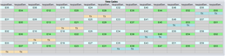
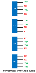
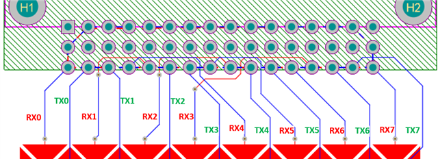
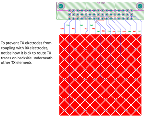
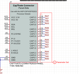
Can you tell me about the connection of the attached 8x8 Touchpad(CapTIvate Touchpad Altium Projects)?
I tried using auto-assign in the design center.
It did not make this connection.
It looks like CAPx.0 and CAPx.3 are RX, and CAPx.1 and PAPx.2 are TX.
Are these pin assignments the result of routing considerations, or are the pin assignments based on some rules?

Best regards,
DDdoor

  • I advice you layout based on the auto pin assignments from GUI. If you just need a 8x8 touchpad, you can assign them by yourself. The only difference is that you will not get the shortest scan cycle like the auto pin assignments. If you want to realize a trackpad, I advise you must follow the auto pin assignments, because it is limited by the software.

  • Hi DDdoor,

    Yes, Eason is correct.  The Captivate design center GUI will choose the optimal connections between the MCU and the sensor.  If you use the GUI's recommended connections, then you must create your PCB layout and routing to match.  Most of the time (especially with touchpads) this is not possible, due to the size of the PCB and other issues making it difficult to route the PCB traces between the MCU and the touchpad. So you have to decide these connections manually.

    There is a procedure for picking the pins in the correct order and is described in a section in the Captivate technology guide.  Although the examples are showing multi element sliders, the same procedure applies to touchpads.

    I'll use and 8x8 touchpad as an example and summarize here:

    The RX pin assignments are important must be made in a specific order starting from block CAP0 through block CAP3.

    1. Always start with CAP0 and choose any pin to be RX0. Next, on CAP1, choose any pin to be RX1.  On CAP2, choose any pin to be RX2 and on CAP3 choose any pin to be RX3.

    2. For RX4 through RX7, repeat step (1) and assign RX4, RX5, RX6 and RX7 to any available pins, starting over with CAP0 through CAP3.

    3. The TX pin assignments don't have any special order.  You can choose any pin on any block for the TX0 through TX7 assignments.  Whatever makes it easiest to route your PCB traces.

    Here is an illustration.

    Do you notice that the diagram you provided follows the same ordering method?

    Here is an example showing the connections on an 8X8 that uses the 48pin connector on the Captivate EVM

    Here is the entire layout. 

**Attention** This is a public forum