This thread has been locked.

If you have a related question, please click the "Ask a related question" button in the top right corner. The newly created question will be automatically linked to this question.

MSP430FR5043: No acknowledgement after slave address

Part Number: MSP430FR5043
Other Parts Discussed in Thread: HDC2022

Hello all,

I'm working on I2C in msp430fr5043. I'm tried to interface with AD5122A (Digital potentiometer). 

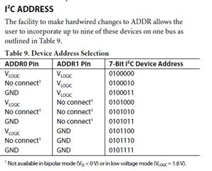
I selected SCLK frequency is 100KHz.  ADDR0 and ADDR1 of AD5122A is connected to GND so according to datasheet of AD5122A, slave address is 0101111.

After start condition and slave address i sent two more bytes to set the potentiometer of 10K ohm is 0x10, 0x0D.

Here the problem is after the start condition UCNACKIFG is set. 

Please find the code below.

#include <msp430.h> 


/**
 * main.c
 */

char array[] = {0x10,0x0D};
int cnt=0;

int main(void)
{
	WDTCTL = WDTPW | WDTHOLD;	// stop watchdog timer
	
	// Software reset enable
    UCB1CTLW0 |= UCSWRST;

    // Clock source selection and SCLK speed
    UCB1CTLW0 |= UCSSEL__SMCLK;
    UCB1BRW = 10;

    //I2C Mode
    UCB1CTLW0 |= UCMODE_3;

    //Master mode
    UCB1CTLW0 |= UCMST;

    //Transmitter mode
    UCB1CTLW0 |= UCTR;

    //Slave address
    UCB1I2CSA = 0x5E;

    //Auto stop
    UCB1CTLW1 |= UCASTP_2;
    UCB1TBCNT = sizeof(array);

    // GPIO Initialization
    P5SEL0 &=~ BIT5;
    P5SEL1 |= BIT5;

    P5SEL0 &=~ BIT6;
    P5SEL1 |= BIT6;

    PM5CTL0 &=~ LOCKLPM5;

    //Disable software reset
    UCB1CTLW0 &=~ UCSWRST;

    //Enable interrupt
    UCB1IE |= UCTXIE0;
    __enable_interrupt();

    int i=0;

    while(1)
    {
        UCB1CTLW0 |= UCTXSTT;

        for(i=0;i<10;i++);

    }

    return 0;
}

#pragma vector = EUSCI_B1_VECTOR
__interrupt void EUSCI_B1_I2C_ISR(void)
{
    if(cnt == sizeof(array)-1)
    {
        UCB1TXBUF = array[cnt];
        cnt=0;
    }

    else
    {
        UCB1TXBUF = array[cnt];
        cnt++;
    }
}


I'm using 

1. MSP430-FR5043 microcontroller

2. MSP430 USB-Debug - Interface (MSP-FET430UIF) for programming.

Please guide me where I'm doing mistake.

Thanks,

Ashok.  

  • >  UCB1I2CSA = 0x5E;

    0b0101111 is 0x2F, so try:

    >  UCB1I2CSA = 0x2F;

    -------------------

    Unsolicited: Issuing a Start (UCTXSTT) during a transaction will break up your transaction (I2C Repeated Start). In your while(1) loop you should wait for each operation to complete before starting another one. This is often done using "LPM0;" in main() matched by an "LPM0_EXIT;" in the ISR when it determines the transaction is finished (e.g. when you set cnt=0). 

  • Hello Bruce,

    Thanks for reply. 

    0b0101111 is 0x2F, so try:

    I tried this way but still it is not solved. and also made following changes.

    while(1)
    {
    UCB1CTLW0 |= UCTXSTT;

    __delay_cycles(4);

    //Enter LPM4 w/interrupts enabled
    __bis_SR_register(LPM0 + GIE);

    //For debugger
    __no_operation();


    }

    In ISR:- 

    if(cnt == sizeof(array)-1)
    {
    UCB1TXBUF = array[cnt];
    cnt=0;
    __bis_SR_register(LPM0_EXIT + GIE);
    }

    else
    {
    UCB1TXBUF = array[cnt];
    cnt++;

    }

    In debugging, after the start command UCNACKIFG becomes set 

    Thanks,

    Ashok.

  • __bis_SR_register(LPM0 + GIE);

    This should be

    __bis_SR_register(LPM0_bits + GIE);

    (or just "LPM0;")

    ------------------

    > __bis_SR_register(LPM0_EXIT + GIE);

    This should be:

    > __bic_SR_register_on_exit(LPM0_bits);

    (or just "LPM0_EXIT;")

    -----------------

    If you're using the correct I2C address, I'm not sure what would cause a NACK. Did it happen on the first byte of the first transaction? (If you have a scope, that's often helpful.)

    Also, what board is the AD5122A installed on? Is it something from ADI?

    -----------------

    More generally, I encourage you to read over the TI Examples. Example map430fr6043_euscib0_i2c_10.c isn't a perfect fit, but will show some of the common practices:

    https://dev.ti.com/tirex/explore/node?node=AL26X3u7yNV4F76.1azaJQ__IOGqZri__LATEST

    -----------------

    Unsolicited:

    > __delay_cycles(4);

    I suggest you remove this line. There's a race here, and this line increases the probability of encountering it. (This would not cause a NACK, but it will cause trouble eventually.)

  • Hello Bruce,

    __bis_SR_register(LPM0 + GIE);

    This should be

    __bis_SR_register(LPM0_bits + GIE);

    (or just "LPM0;")

    ------------------

    > __bis_SR_register(LPM0_EXIT + GIE);

    This should be:

    > __bic_SR_register_on_exit(LPM0_bits);

    (or just "LPM0_EXIT;")

    I made changes and tested but problem is not solved. 

    If you're using the correct I2C address, I'm not sure what would cause a NACK. Did it happen on the first byte of the first transaction? (If you have a scope, that's often helpful.)

    To find that i changed code as mentioned below

    #include <msp430.h> 
    
    char array[] = {0x10,0x0D};
    int cnt=0;
    
    int main(void)
    {
    	WDTCTL = WDTPW | WDTHOLD;	// stop watchdog timer
    	
    	// Software reset enable
        UCB1CTLW0 |= UCSWRST;
    
        // Clock source selection and SCLK speed
        UCB1CTLW0 |= UCSSEL__SMCLK;
        UCB1BRW = 10;
    
        //I2C Mode
        UCB1CTLW0 |= UCMODE_3;
    
        //Master mode
        UCB1CTLW0 |= UCMST;
    
        //Transmitter mode
        UCB1CTLW0 |= UCTR;
    
        //Slave address
        UCB1I2CSA = 0x5E;
    
        //Auto stop
        UCB1CTLW1 |= UCASTP_2;
        UCB1TBCNT = sizeof(array);
    
        // GPIO Initialization
        P5SEL0 &=~ BIT5;
        P5SEL1 |= BIT5;
    
        P5SEL0 &=~ BIT6;
        P5SEL1 |= BIT6;
    
        PM5CTL0 &=~ LOCKLPM5;
    
        //Disable software reset
        UCB1CTLW0 &=~ UCSWRST;
    
        //Enable interrupt
       // UCB1IE |= UCRXIE0 | UCTXIE0;
        //__enable_interrupt();
    
        int i=0;
    
        while(1)
        {
            UCB1CTLW0 |= UCTXSTT;
    
            if(UCB1IFG & UCNACKIFG)
            {
               // UCB1CTLW0 |= UCTXSTT;
            }
    
            else
            {
                if(UCB1IFG & UCTXIFG)
                {
                    if(cnt <= sizeof(array)-1)
                        {
                            UCB1TXBUF = array[cnt];
                            cnt++;
                        }
    
                }
            }
        }
    
         return 0;
    }


    And i found out that after the slave address I'm getting no acknowledgement.

    if i given slave address as 0x5e then in the oscilloscope shown as 0xBC including no acknowledgement.

    SCL :   1      2     3      4      5      6      7     8 (r/w)     9 (ack)

    SDA:    1      0     1      1      1      1      0     0             1

    Similarly, when i given slave address is 0x2F then in oscilloscope shown as 0x5E including no acknowledgement.

    SCL :   1      2     3      4      5      6      7     8 (r/w)     9 (ack)

    SDA:    0      1     0      1      1      1      1     0             1

    After start condition slave address which is written in the code is left-shifted by 1 and 0th bit is taken as 0 due to writing. 

    But in the both cases the ninth clock bit is one. Is my initialization of I2C is correct or anything i forgot?

    Also, what board is the AD5122A installed on? Is it something from ADI?

    This is customized board which includes Msp430fr5043, AD5122 (Digital potentiometer) by Analog devices. There are three slave devices are hang on the I2C bus and AD5122 is one of the slave device.

    Please guide me where I'm doing mistake.

    Thanks,

    Ashok. 

  • Is it possible /RESET (pin 2) is being held low?

    Can you get to the other I2C devices on the bus?

  • Hello Bruce,

    Is it possible /RESET (pin 2) is being held low?

    I didn't understand the question.

    Can you get to the other I2C devices on the bus?

    I tried with another I2C slave device of hdc2022 still I'm not got the acknowledgement. 

  • Check your board's schematic to see what the /RESET pin (2 or 16, depending on the package) of the AD5122A is connected to. If it's being held low (GND) I expect the device won't respond. The data sheet recommends tying it to Vlogic if you're not using it.

    If you can't get to any of the (other) devices on your I2C bus, that sounds electrical, so check your wiring.

  • Hello Bruce,

    Check your board's schematic to see what the /RESET pin (2 or 16, depending on the package) of the AD5122A is connected to. If it's being held low (GND) I expect the device won't respond.

    Reset pin  of AD5122 is connected to Vcc. 

    If you can't get to any of the (other) devices on your I2C bus, that sounds electrical, so check your wiring.

    I will check on it. 

    Thanks,

    Ashok.

  • Hi Lakkoji,

    Does this issue have been resolved?

    Thanks!

    Best Regards

    Johnson 

  • Hello Bruce,

    I verified the board and there is wiring issues this might be reason for not got acknowledgement.

    And also i verified with another slave device it is got the acknowledgement.

    But the problem is I'm unable to see the SCL and SDA signals in the oscilloscope.

  • Hello Johnson,

    Yes, I tried with another slave in the bus i got the acknowledgement but i'm unable to see the SCL and SDA. i.e. SCL is LOW and SDA is high all the time.

    I interface  EEPROM of AT24CM02 with msp430 fr-5043.

    Address of slave is 1010 a2 address adr16 r/w --> I written as 0X50 (A2 is connected to ground.)

    Please check code below

    #include <msp430.h> 
    #include"stdio.h"
    
    char array[]={0x00,0x00,0x12};
    char array_2[]={0x00,0x00};
    
    int cnt=0;
    
    int main(void)
    {
    	WDTCTL = WDTPW | WDTHOLD;	// stop watchdog timer
    	
    
    	    CSCTL0_H = CSKEY_H;                                                 // Unlock CS registers
    	    CSCTL1 = DCOFSEL_3 | DCORSEL;                                       // Set DCO to 8MHz
    	    CSCTL2 = SELA__VLOCLK | SELS__DCOCLK | SELM__DCOCLK;
    	    CSCTL3 = DIVA__1 | DIVS__1 | DIVM__1;                               // Set all dividers
    	    CSCTL0_H = 0;                                                       // Lock CS registers
    
    	// GPIO Initialization
    	    P5SEL0 &=~ BIT5;            // SDA
    	    P5SEL1 |= BIT5;
    
    	    P5SEL0 &=~ BIT6;            //SCL
    	    P5SEL1 |= BIT6;
    
    	    P5DIR |= BIT6;
    
    	    PM5CTL0 &=~ LOCKLPM5;
    
    	// Software reset enable
        UCB1CTLW0 |= UCSWRST;
    
        // Clock source selection and SCLK speed
        UCB1CTLW0 |= UCSSEL__SMCLK | UCSWRST;
        UCB1BRW = 160;
    
        //I2C Mode
        UCB1CTLW0 |= UCMODE_3;
    
        //SYNC
        UCB1CTLW0 |= UCSYNC;
    
        //Master mode
        UCB1CTLW0 |= UCMST;
    
        //Transmitter mode
        UCB1CTLW0 |= UCTR;
    
        //Slave address
        UCB1I2CSA = 0x50;     
    
        //Auto stop
        UCB1CTLW1 |= UCASTP_2;
        UCB1TBCNT = sizeof(array);
    
        //Disable software reset
        UCB1CTLW0 &=~ UCSWRST;
    
        //Enable interrupt
       // UCB1IE |= UCRXIE0 | UCTXIE0;
        //__enable_interrupt();
    
        int i=0;
    
        while(1)
        {
            UCB1CTLW0 |= UCTXSTT;
    
            if(UCB1IFG & UCNACKIFG)
                {
                   // UCB1CTLW0 |= UCTXSTP;
                }
    
            else
                {
                    while(cnt <= sizeof(array)-1)
                            {
                                while(!(UCB1IFG & UCTXIFG0));
                                UCB1TXBUF = array[cnt];
                                cnt++;
    
                            }
    
                        cnt=0;
                        __delay_cycles(8000000);
    
                        UCB1CTLW0 |= UCTR;
                        UCB1TBCNT = sizeof(array_2);
                        UCB1CTLW0 |= UCTXSTT;
    
    
                        while(cnt <= sizeof(array_2)-1)
                            {
                                 while(!(UCB1IFG & UCTXIFG0));
                                 UCB1TXBUF = array_2[cnt];
                                 cnt++;
    
                            }
                        UCB1CTLW0 &=~ UCTR;
                        UCB1TBCNT =1;
                        UCB1CTLW0 |= UCTXSTT;
                        while(!(UCB1IFG & UCRXIFG));
                        rcv = UCRXBUF;
    
                    }
    
    
            }
    
        
        return 0;
    }


    While debugging, I'm not getting any no NACK flag and also writing the value = 0x01 at address of 00 00000000 00000000 but I'm unable to see the SDA and SCL and also while reading data from eeprom i got oxff instead of 0x01.

    Please guide me where I'm doing mistake.

    Thanks,

    Ashok.

  • 1) If SCL is low ("stretched") all the time, the bus is hung since the master can't issue a Start (nor Stop). This could be caused by any of the devices on the bus (including the master). Check your SCL pullup (again) and power-cycle the whole system to clear it up. (It's possible this condition was triggered by some of your earlier experiments.)

    2) UCB1TBCNT can only be changed while the I2C is in reset (UCSWRST=1) [Ref User Guide (SLAU367P) Table 32-8]. Yes, this is a bit of a bother. What this means is that your 2nd (of 3) transaction leaves the address pointer at 0x0001, but you only wrote address 0x0000. (The EEPROM is initially filled with 0xFF.)

    3) UCNACKIFG won't be set as early as you're checking it, since the I2C unit has had no time to send the address byte. Per the UG (Fig 32-12) it isn't set until after your first write to TXBUF.  (I think I've seen it earlier than that, but not by much.)

  • Hello Bruce,

    Check your SCL pullup (again) and power-cycle the whole system to clear it up. (It's possible this condition was triggered by some of your earlier experiments.)

    SCL pull -up resistor is 4.7K ohm according to at24cm02 pull up resistor is maximum 10k ohm. What is meant by power cycle whole system to clear it up ? I reset the board, Flash the another code of toggle a pin and re-flash i2c code but all these not resolved the problem.

    UCB1TBCNT can only be changed while the I2C is in reset (UCSWRST=1) [Ref User Guide (SLAU367P) Table 32-8]. Yes, this is a bit of a bother.

    Done as per your suggestion but problem is unresolved.

    -------------------------------------------------------------------------------------------------------------------------------------------------------------------------------

    After I2C initialization (after clear software reset) UCBUSY is set and all the flags are zero including (UCTXIFG). 

    SCL and SDA is high. 

    After going through this post 

    https://e2e.ti.com/support/microcontrollers/msp-low-power-microcontrollers-group/msp430/f/msp-low-power-microcontroller-forum/625641/msp430f5529-i2c-stuck-waiting-for-uctxifg

    I modified the code and tested 

    #include <msp430.h> 
    #include"stdio.h"
    
    char array[]={0x00,0x01,0x04};
    char array_2[]={0x00,0x01};
    char rcv=0;
    char uart[5]={0};
    
    int cnt=0,i=0;
    
    void toggle_busy()
    {
       // UCB1CTLW0 |= UCTXSTP;
    
        P5SEL0 = 0X00;
        P5SEL1 = 0x00;
    
        P5REN |= 0X60;
    
        P5DIR |= 0X60;
    
        P5OUT |= 0X60;
    
        for(i=0;i<10;i++)
        {
            P5OUT &=~ 0x60;
            __delay_cycles(1000000);
            P5OUT |= 0x60;
            __delay_cycles(1000000);
        }
    
        // GPIO Initialization
    
            P5REN &=~ 0X60;
    
            P5DIR &=~ 0X60;
    
            P5SEL0 &=~ BIT5;            // SDA
            P5SEL1 |= BIT5;
    
            P5SEL0 &=~ BIT6;            //SCL
            P5SEL1 |= BIT6;
    
            //UCB1CTLW0 |= UCTXSTT;
            if(UCB1STATW & UCBBUSY)
            {
                toggle_busy();
            }
    }
    
    int main(void)
    {
    	WDTCTL = WDTPW | WDTHOLD;	// stop watchdog timer
    	
    
    	    CSCTL0_H = CSKEY_H;                                                 // Unlock CS registers
    	    CSCTL1 = DCOFSEL_0 | DCORSEL;                                       // Set DCO to 1MHz
    	    CSCTL2 = SELA__VLOCLK | SELS__DCOCLK | SELM__DCOCLK;
    	    CSCTL3 = DIVA__1 | DIVS__1 | DIVM__1;                               // Set all dividers
    	    CSCTL0_H = 0;                                                       // Lock CS registers
    
    
    	    //------------------------------------------CHANGES MADE HERE -----------------------------------------//
    //	    P5SEL0 &=~ 0X60;
    //	    P5SEL1 &=~ 0X60;
    
    	    P5SEL0 &=~ BIT5;
    	    P5SEL1 &=~ BIT5;
    
    	    P5SEL0 &=~ BIT6;
    	    P5SEL1 &=~ BIT6;
    
    
    	    P5REN |= BIT6;
    	    P5REN |= BIT5;
    
    	    P5DIR |= BIT5;
    	    P5DIR |= BIT6;
    
    	    P5OUT |= BIT6;
    	    P5OUT |= BIT5;
    
    
    	    //-------------------------------------------CHANGES END HERE-----------------------------------------//
    
    	// Software reset enable
        UCB1CTLW0 |= UCSWRST;
    
        // Clock source selection and SCLK speed
        UCB1CTLW0 |= UCSSEL__SMCLK | UCSWRST;
        UCB1BRW = 10;
    
        //I2C Mode
        UCB1CTLW0 |= UCMODE_3;
    
        //SYNC
        UCB1CTLW0 |= UCSYNC;
    
        //Master mode
        UCB1CTLW0 |= UCMST;
    
        //Transmitter mode
        UCB1CTLW0 |= UCTR;
    
        //Single master
        UCB1CTLW0 &=~ UCMM;
    
        //Slave address
        UCB1I2CSA = 0x50;     //0x23 or 0x2f for pot and 0x50 for eeprom ;
    
        //Auto stop
        UCB1CTLW1 |= UCASTP_2;
        UCB1TBCNT = sizeof(array);
    
        //Disable software reset
            UCB1CTLW0 &=~ UCSWRST;
    
            // GPIO Initialization
    
                    P5REN &=~ BIT6;
                    P5REN &=~ BIT5;
    
                    P5DIR &=~ BIT5;
                    P5DIR &=~ BIT6;
    
                    P5OUT &=~ BIT6;
                    P5OUT &=~ BIT5;
    
                    P5SEL0 &=~ BIT5;
                    P5SEL1 |= BIT5;
    
                    P5SEL0 &=~ BIT6;
                    P5SEL1 |= BIT6;


            if(UCB1STATW & UCBBUSY)
                  {
                      toggle_busy();
                  }
    
    
        while(1)
        {
               // UCB1CTLW0 |= UCTXSTP;
                UCB1CTLW0 |= UCTXSTT;


                if(UCB1IFG & UCNACKIFG)
                {
                   // UCB1CTLW0 |= UCTXSTP;
                }
    
    
                else
                {
    2               // UCB1CTLW0 |= UCTXSTP;
    
    
                        while(cnt <= sizeof(array)-1)
                            {
                                while(!(UCB1IFG & UCTXIFG0));
                                UCB1TXBUF = array[cnt];
                                cnt++;
    
                            }
    
                       // UCB1CTLW0 |= UCTXSTP;
                        cnt=0;
                        __delay_cycles(8000000);
    
                }
    
    
            }
    
        return 0;
    }


    In my case still UCBBUSY is not clear.

    Please guide me.

    Thanks,

    Ashok

  • Hi Ashok,

    Does this thread have been resolved, or need other support? 

    Thanks!

    Best Regards

    Johnson

**Attention** This is a public forum