Hi Experts!
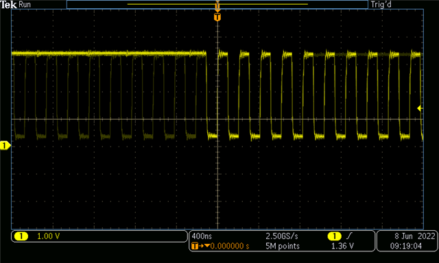
I'm probing PJ.2 to view ADC10CLK and the waveform is not as expected. Any ideas why this is?
1) I'm not using the debugger. (Using debugger previously made 8 MHz MCLK look strange)
2) MCLK looks perfect when probing J.0
3) SMCLK shares the same odd behavior as ADC10CLK when probing J.1
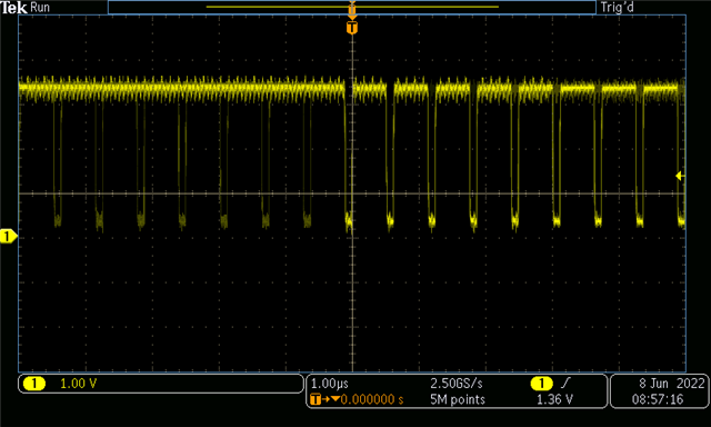
4) There is jitter seen on the zoomed out scope capture.
ADC10CLK (PJ.2) Scope Capture zoomed out:
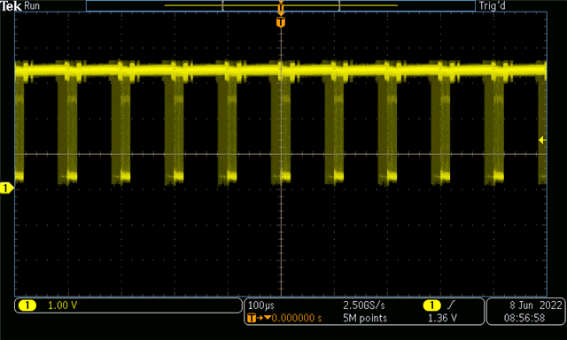
ADC10CLK (PJ.2) Scope Capture zoomed in. The left half flickers on/off:
Attached is the relevant code:
// MSP430F51x2
// -----------------
// /|\| |
// | | |
// --|RST |
// GPIO to trip relay <-- (1)|P1.0 PJ.0 | (7) --> SMCLK (debug)
// AC + DC >---(2)|P1.1/A1 PJ.1 | (8) --> MCLK (debug)
// GPIO to debug TimerA <-- (4)|P1.3 PJ.2 | (9) --> ADC10CLK (debug)
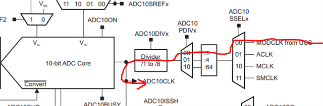
PJSEL |= BIT0 + BIT1 + BIT2; //Output CLKs to PJ.0-2
PJDIR |= BIT0 + BIT1 + BIT2;
// configure clocks
UCSCTL3 = SELREF_2; // Set DCO FLL reference = REFO
UCSCTL4 |= SELA_2; // Set ACLK = REFO
__bis_SR_register(SCG0); // Disable the FLL control loop
UCSCTL0 = 0x0000; // Set lowest possible DCOx, MODx
UCSCTL1 = DCORSEL_5; // Select DCO range 16MHz operation
UCSCTL2 = FLLD_1 + 243; // Set DCO Multiplier for 8MHz
// (N + 1) * FLLRef = Fdco
// (243 + 1) * 32768 = 8MHz
__bic_SR_register(SCG0); // re-enable the FLL control loop
// Worst-case settling time for the DCO when the DCO range bits have been
// changed is n x 32 x 32 x f_MCLK / f_FLL_reference. See UCS chapter in 5xx
// UG for optimization.
// 32 x 32 x 8 MHz / 32,768 Hz = 250000 = MCLK cycles for DCO to settle
__delay_cycles(250000);
// Loop until XT1 & DCO stabilizes - In this case only DCO has to stabilize
do
{
UCSCTL7 &= ~(XT1LFOFFG + XT1HFOFFG + DCOFFG);
// Clear XT1,DCO fault flags
SFRIFG1 &= ~OFIFG; // Clear fault flags
}while (SFRIFG1&OFIFG); // Test oscillator fault flag
P1DIR |= BIT0 +BIT3; // Set P1.0, P1.3 output direction
P1OUT &= ~BIT0; // Clear P1.0
// Configure internal reference
while(REFCTL0 & REFGENBUSY); // If ref generator busy, WAIT
REFCTL0 |= REFVSEL_0+REFON; // Select internal ref = 1.5V
// Set FSR of ADC10 for ADC10SREF
__delay_cycles(100); // Delay for Ref to settle
// Configure ADC10
ADC10CTL0 &= ~ADC10ENC; // Disable ADC
ADC10CTL0 |= ADC10SHT_2; // clk cycles per sample period
ADC10CTL0 |= ADC10ON; // enable ADC10
ADC10CTL1 |= ADC10SSEL_0; // ADC clock = MODCLK = 5MHz
ADC10CTL1 |= ADC10SHP; // pulse sample mode
ADC10CTL1 |= ADC10CONSEQ_0; // single-conversion, single-channel mode 27.2.7
ADC10CTL1 |= ADC10SHS_0; // triggered sample with ADC10SC
ADC10CTL2 |= ADC10RES; // 10-bit conversion results
ADC10MCTL0 = 0;
ADC10MCTL0 |= ADC10SREF_1; // (REF_x) V+ = Vref+, V- = AVSS
ADC10MCTL0 |= ADC10INCH_1; // Read ch 1 (P1.1)
ADC10IE |= ADC10IFG0; // Interrupt enable
ADC10CTL0 |= ADC10ENC + ADC10SC; // Enable ADC and trigger ADC read