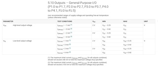
Outputs – General-Purpose I/O (P1.0 to P1.7, P2.0 to P2.7, P3.0 to P3.7, P4.0 to P4.1, PJ.0 to PJ.5) what is the absolute max current can sink and source for one of those pins?
is there a hardware data sheet that supports hardware design?
Outputs – General-Purpose I/O (P1.0 to P1.7, P2.0 to P2.7, P3.0 to P3.7, P4.0 to P4.1, PJ.0 to PJ.5) what is the absolute max current can sink and source for one of those pins?
is there a hardware data sheet that supports hardware design?
**Attention** This is a public forum