This thread has been locked.

If you have a related question, please click the "Ask a related question" button in the top right corner. The newly created question will be automatically linked to this question.

TIDM-3PHMTR-TAMP-ESD: MSP430F67791AIPEU

Part Number: TIDM-3PHMTR-TAMP-ESD

Hello Team,

To protect ADC pins of MCU, clamping diodes are essential. If the input voltage of an ADC pins is maximum of let us say, 3.6V, the clamping diode of 0.2V to 0.3V should be used when the diode is connected between ADC pin and 3.3V source.

Is my understanding right?

In reference design available in the design guide TIDM-3PHMTR-TAMP-ESD there are two PMLL4148 whose forward voltage (Vf) is 0.7V used in the current sensing section. Total voltage drop is 1.4V across 2 diodes. Which means ADC pin is clamped at 4.7V which could damage microcontroller. 

Shall i use one Schottky with 0.2V forward drop in place of 2 PMLL4148 diodes to protect MSP controller with 3.5V clamping at ADC pin?

If not, please explain the reason for 2 PMLL4148 for clamping.

  • Hello Maha,

    I'm looking into your request now and will provide feedback tomorrow.

    Thank you for your patience!

    BR

  • Hi again,

     The two in series PMLL4148 diodes are used to allow for full scale signal swing (FSR) at the MSP430 inputs while limiting the max. voltage to a safe level (see Abs. ratings). This circuitry has been tested and proven to achieve Class 0.2 E-meter accuracy.

    Here is the detailed explanation: In the TID Design guide — TIDM-3PHMTR-TAMP-ESD you will find:

    3.2.1 Analog Inputs

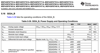
    The MSP430 analog front end consists of ΣΔ ADCs. Each converter is differential and requires that the input voltages at the pins does not exceed ±930 mV (gain = 1) for optimum results. To meet this input voltage specification, the current and voltage inputs must be divided down. In addition, the SD24 allows a maximum negative voltage of −1 V; therefore, AC signals from mains can be directly interfaced without the need for level shifters. This sub-section describes the analog front end used for voltage and current channels.

    This text relates to the MSP430 Datasheet numbers for SD24_B module:

    The TIDM-3PHMTR-TAMP-ESD UG says in Ch.3.2.1.2: 

    3.2.1.2 Current Inputs

    The analog front-end for current inputs is slightly different from the analog front end for the voltage inputs. Figure 7 shows the analog front end used for a current channel. The analog front end for current consists of diodes and transorbs for transient voltage suppression. In addition, the front-end consists of EMI filter beads (which help for ESD testing), burden resistors for current transformers, and also an RC low-pass filter that functions as an anti-alias filter.

    …As Figure 7 shows, resistor R21 is the burden resistor selected based on the current range used and the turns ratio specification of the CT (this design uses CTs with a turns ratio of 2000:1). The value of the burden resistor for this design is around 13 Ω. The antialiasing circuitry, consisting of resistors and capacitors, follow the burden resistor. Based on this EVMs maximum current of 100 A, CT turns ratio of 2000:1, and burden resistor of 13 Ω, the input signal to the converter is a fully differential input with a voltage swing of ±919 mV maximum when the maximum current rating of the meter (100 A) is applied. In addition, footprints for suppressant inductors are also available. Figure 7 shows these inductor footprints as R/L9 and R/L10, which are populated by default with 0-Ω resistors.

    So, R21 and the CT used already limit the Input voltage to acceptable levels for the MSP430 device. But in case of overvoltage event you want to make sure that this voltage does not damage the MSP430. So having +- 1000mV is OK but going beyond AVCC is not allowed and this is exactly the role of the PMLL4148 devices.

    To maximize accuracy, we want to use the MSP430 full input range of +-930mV by scaling the current transformer’s burden resistor accordingly.  If you only use one diode, the input signal to the ADC would get clamped somewhere between ±500-700 mV, which does not allow for getting accurate results at higher input currents (>50 Amps).

    To deal with this, we use two diodes in series (so clamping will be at ±1000-1400mV), which prevents the waveform from being clamped at higher currents while still using the full input range of F67xx without using the internal PGA.

  • Hi Milen,
    Thank you for your response.
    Due to power concern, in my case I am using 2mohm shunt for measuring maximum load of 40A.
    116mV will be the maximum differential voltage applied at ADC pins. ADC Gain is set to 8.
    So, according to your explanation, there is no problem in providing one diode which could clamp at 500mV in my case. Is it correct?

**Attention** This is a public forum