This thread has been locked.
If you have a related question, please click the "Ask a related question" button in the top right corner. The newly created question will be automatically linked to this question.
I'm trying to configure PGA302(slave) using MSP430FR5969 (master) launchpad through I2C protocol. I want to set the P Gain so the input voltage is amplified according to the gain. I'm giving input voltage to VINPP and VINPN pins and checking the output on Vout terminal. I have connected P1.6 (SDA) to pin 13 and P1.7 (SCL) to pin 14. I'm giving VDD of 5V to PGA302. I have grounded the VINTP and VINTN.I have connected common ground to both the devices.
In the CCS code, I am putting the PGA302 in reset mode by sending 0x03 to register address 0x0C of slave address 0x40. Then I set the P gain by sending 0x01(for gain of 2 V/V). And finally I take out the slave from reset mode by sending 0x00 to register address 0x0C of slave address 0x40. I am using the polling mode(checking the flag is cleared for Tx buffer to be ready).
I'm unable to view the waveform of SDA and SCL in oscilloscope. Differing the P Gain Value doesn't change the Vout value. I can see the TXBUF is getting the values I'm sending, so I assume the slave is responding.
Am I missing some steps or is there an issue with the connection? If possible please provide a sample code for I2C communication of MSP430FR5969 to set the P Gain of PGA302.
Hi,
I think below links will give you some guidance:
I'm unable to view the waveform of SDA and SCL in oscilloscope
Make sure you have pull-up resistor in SCl/SDA line on the board.
B.R.
Sal
Hi,
I'm unable to see the SCL and SDA waveforms using these codes. Also, these codes are not that easy to comprehend. I'm not getting any data in Rx buffer while reading from a specific register. Energia codes for the same would be an easy approach. Can I get the sample code for that?
Hi,
There should be some waveforms (Start signal and write address signal) if you configure MCU properly even if there is no slave.
Energia is the third party development environment for MSP quick runing and evaluation. And Energia is no longer maintained by TI.
B.R.
Sal
The PGA3 people don't seem to have much to say about this device. 43oh seems to be deserted.
energia.nu still seems to be live. I don't see evidence of an Arduino/Energia library for the PGA302. mikroe.com sells a "Click" board with a PGA302 on it; they may have some relevant software.
There are people here that might be able to help from First Principles. But you need to give us some clues.
1) What is your platform? EVM+Launchpad? How are they wired?
2) What code are you using?
3) How do you tell that you've (successfully) written registers 0x40/0x0C and 0x42/0x47? Readback? Scope trace?
The EVM has an MSP430 on it, but the last I saw, TI won't release the firmware. Which really limits the usefulness of the EVM.
According to the EVM book (SLDU031), that's an F5510 (not FR5969) running USB2ANY; I didn't know USB2ANY was secret, but I think it's for the GUI so they probably don't intend for people to mess with it anyway.
Yes, but the F5510 is sending all the GUI stuff to the PGA302, by I2C *or* OWI. This communication code would be very handy for a developer.
I expect USB2ANY uses ordinary MSP430 I2C code, which is arcane but not inscrutable. I'm not sure seeing it would be all that informative.
What's opaque (to me) is the register setup -- which registers need to be set to what to actually accomplish anything. The GUI seems to be the one that knows this [Ref EVM UG Fig 23]. The GUI is also Object-Code-Only.
Anyway, I don't mean to hijack this thread. Maybe the Original Poster has already solved everything.
No, I haven't been able to solve the issue till now.
I'm using PGA302 as slave and MSP430FR5969 launchpad as master to configure the slave through I2C.
I'm currently trying out the following code to write on the P_GAIN_SEL register:
#include <Wire.h>
#define PGA302_ADDRESS 0x42 // PGA302 I2C address
void setup() {
Wire.begin(); // Initialize I2C communication
Serial.begin(9600); // Initialize serial communication
}
void loop() {
// Set PGA302 into reset mode
setResetMode(true);
// Configure PGA302 settings (e.g., set P gain)
setPGAGain(0x02); // for gain=4
// Take PGA302 out of reset mode
setResetMode(false);
// Monitor PGA302 output
// Code to read and monitor PGA302 output goes here
delay(1000); // Delay for demonstration purposes
}
void setResetMode(bool mode) {
Wire.beginTransmission(0x40);
Wire.write(0x0C); // Register address for RESET_MODE (adjust if necessary)
Wire.write(mode ? 0x03 : 0x00); // Set/reset mode bit
Wire.endTransmission();
}
void setPGAGain(uint8_t gain) {
Wire.beginTransmission(PGA302_ADDRESS);
Wire.write(0x47); // Register address for P_GAIN_SELECT (adjust if necessary)
Wire.write(gain); // Set P gain value
Wire.endTransmission();
}
I saw a post that explained that PGA302 has to be put in reset mode first to access registers other than test registers. And it has to be taken out of reset mode to see the actual Vout.
But I don't think the values are being written on the register because when I read back the register it constantly shows 255 (any register I read). Normally, even if I don't write anything, it should be 0. I have connected pin 14 (of PGA302) to P3.5 (SCL) of launchpad and pin 13 (of PGA302) to P3.6 (SDA) of launchpad. Rest all the connections are the same as mentioned in the original post.
I was also trying to work on the PGA302EVM but the same problem was occurring.. Even after writing directly in the register, no change in Vout was observed.
The Arduino Wire.read() returns 0xFF (really -1) if available()==0, e.g. if the requestFrom() failed. You might want to check the result from Wire.endTransmission() to see if the writes are failing as well.
It sounds as though you're (now) not using the EVM. What platform are you using? I'm asking since some commercial breakout boards include the I2C pullups and some don't. The Launchpad itself doesn't. If you don't have a scope, a voltmeter applied to the SCL/SDA pins might tell you something.
I'm just using the PGA302 standalone IC with MSP430FR5969 launchpad. I have also connected 5k pull up resistors on the SDA and SCL lines. I do have a scope but I'm unable to comprehend the waveforms. After the start bit (SDA pulled low), the slave address 0x40 has to be sent but like is the line high or low at 4? like will be LHLL LLLL or HLHH HHHH?
The code looks fine as far as it goes. I suspect the failure is elsewhere. Can you see the ACK/NACK bit in your scope trace?
If you're working with a bare chip, how are you handling the 3V/5V translations? Can you tell whether the chip is powering up?
More generally: Is there a reason you're not using your EVM? I expect the EVM is built to sidestep a number of startup problems, so you can solve things one at a time.
I used this code (provided by someone in my other post) and now I'm able to read and write on registers. I'm yet to try writing on the P_GAIN_SELECT register and observe the change in Vout.
In the EVM, no change was observed even by changing the values in registers. Assuming it directly gets programmed into the PGA302, it should have worked. Or are there any other registers that need to be changed? I'll also check the value stored in PADC registers.
Also, the EVM just randomly stopped working ( unable to detect through USB), so I have no other option than to just use the IC.
I don't know what other setup is required to get the device going. Looking at data sheet Tables 11 and 14, it's possible it was designed to produce something at Vout as soon as it's powered up. Can you measure anything for that case?
Do you need to have a bridge attached in order to get Vout? The EVM (out of the box) seems to have a "Bridge Emulator" connected via J5-7. You might be able to tap into that (even without the USB) using the jumper pins [Ref EVM UG Fig 6].
Another clue might be in EVM User Guide Fig 23. This shows (we suppose) an actual configuration sequence. I count only 7 transactions (register settings); it might be worth figuring out what those are to see if you need to do any of them.
As for the USB: The EVM UG says that the F5510 MCU is running USB2ANY firmware. USB2ANY is also a separate TI product (using an F5529, I think); it might be worth a search of the Forum to see if other USB2ANY users have encountered the USB suddenly failing.
I have attached an external Wheatstone bridge that gives out a differential output of 0.5V to connect to VINPN and VINPP pins(giving excitation voltage from VBRGP and VBRGN). The Bridge emulator on EVM doesn't give an appropriate differential voltage. Even when the EVM was working, changing the digital resistor's value using GUI didn't change the differential voltage.
The sequence shown in the figure doesn't signify anything. As to access registers from DI page address 0x02 (slave adress=0x42), the device must be in reset mode (0x03 in 0x0C of 0x40), but according to the command, it was in running mode. Also, most of the registers configured after that aren't even mentioned in the datasheet (ex: there is no mention of register 0x67 in 0x42 slave).
If you just power up the device and don't do anything (with your bridge attached) do you see anything on Vout? (I suppose it would be about 1.3*0.5=~0.6V.) Do you see any bridge excitation?
One fairly standard exercise I do after I establish communication with a new device is just read all the registers, comparing them with the Reset values in the data sheet.
I get 4.5V even when VINPN and VINPP are not connected. But it keeps changing without any changes made to the connections.
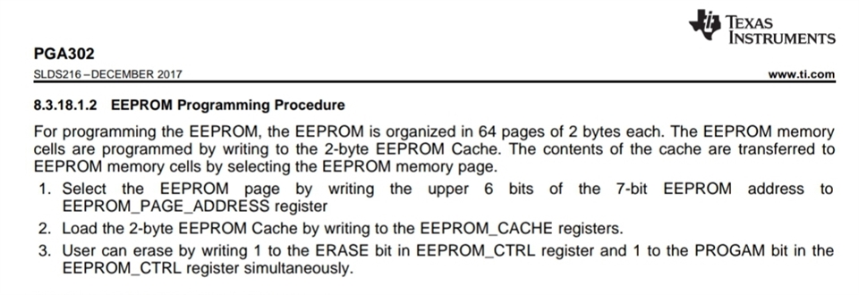
I'm thinking of directly programming the EEPROM P_GAIN_SELECT register. But the steps given in the datasheet given for doing so are a bit confusing. It says to write the upper 6bits of 7bit EEPROM address but the adress of P_GAIN_SELECT is 0x40000026. How is this a 7 bit address? I'm assuming in the 2 byte EEPROM cache first we have to send the last two bits of EEPROM address(0x26 in this case) and then the data we want to store in it. I guess it's supposed to be reflected in the digital interface(i.e., in 0x47 of 0x42). Or how else do we read back the P gain?
I'm a bit suspicious of this description, not least since it looks self-contradictory.
I think it's not an accident that EEPROM_CACHE[],EEPROM_PAGE_ADDRESS, and EEPROM_CTRL are consecutive. My guess is that you should write (maybe as a single transaction): 0x80, data1, data0, address(=0x26), Program(=0x01). I suppose to set a single byte (data1) you would use two transactions: (1) 0x80,data1 (2) 0x82, address, Program. Or maybe you always have to write 2 bytes (knowing ahead of time what the second byte is).
Data sheet Sec 7.19 says the EEPROM write takes 8ms.
I think I read in one of the Forum threads here that the idea is you write the EEPROM in Reset, then when you take it out of Reset the EEPROM gets loaded into the register.
----------------
You probably already saw this but MikroE has a Github repository for their PGA302 Click board. It was somewhat enlightening, but didn't answer all the questions (including this one):
https://github.com/MikroElektronika/mikrosdk_click_v2/tree/master/clicks/loadcell3
I feel like the 0x26(register address for P_GAIN_SELECT in EEPROM) goes into 0x80 and then the data we wanna store(ex: 0x01 for 2V/V gain) goes into 0x81. And for the page address the first 6 bits of 0x40000026 can be 010000 (converting the hex address to binary), so maybe in 0x82 goes 0x10. And then 0x01 in 0x83. But the order has to be 0x82 ->0x80 -> 0x81 -> 0x83 to follow the chronology of a typical I2C write operation (slave address-> register address ->data). What do you think?
Also, then if the value gets stored in the register after you take it out of reset, I have to again set it in reset to see the value in 0x47 of 0x42? So, it's like RESET-> Programming the EEPROM-> RUNNING-> RESET-> Read the corresponding register?
I'm still yet to understand the flow of the sequence, like VINPN and VINPP pins go to P GAIN PGA then there's a ADC and then DAC (some sensor compensation, IIIR filter in between that). So, the value of PADC is the 2's complement of the value at Vout? And the DAC has a buffer gain of 4V/V and it's reference voltage is 0.25*Vddp(Pg: 10 of the datasheet). What exactly is Vddp? Honestly, it's so confusing, and there's no proper explanation of the sequential flow.
All the EEPROM addresses have 0x40 as the high byte, so I don't see how putting that into the EEPROM_PAGE_ADDRESS provides any information. I suppose if one is accustomed to counting bits from the right (low bit is bit-0) calling the low-order bits "first" is natural. (Either way it seems an unfortunate choice of words.)
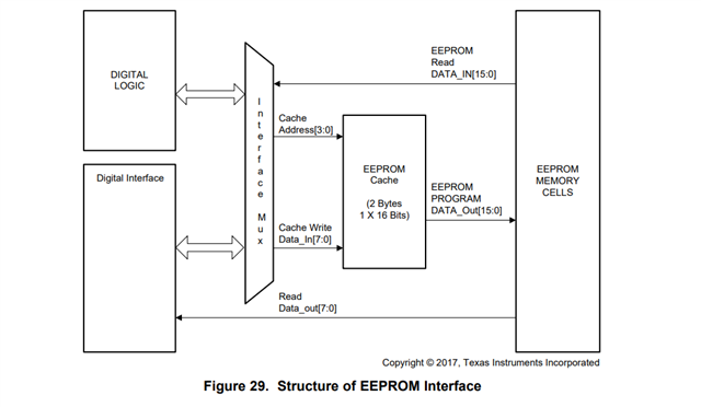
Data sheet Sec 7.19 refers to a "2-byte page", and Fig 29 shows a 16-bit path out to the EEPROM array. That's where my equivocation about trying to write a single byte (the norm for most EEPROMs I'm familiar with) came from. You might find that you have to (re)write one of the neighboring bytes as well.
--------
I got the EEPROM-load cycle description from here:
I'm still scratching my head over how you can ever change the "live" value of a parameter (at least one that has an EEPROM default value). Maybe no one ever does that in practice?
-------
I'm also still stuck on EVM UG Fig 23, even though you've explained it already. It still seems possible that it's an actual configuration sequence, since otherwise why would the authors have hand-typed it?
One of the two undocumented register writes (0x38) is apparently to DAC_CTRL_STATUS; I haven't found an explanation for (0x67).
Then we're left with your observation that (apparently) the configuration happens while the device is Not in Reset (0x42/0x47 is 0x00). Maybe the prohibitions on writing other pages aren't really enforced? Maybe that's actually the way "live" updates are done? (I suspect only the GUI knows this.)
------
I don't have one of these devices. (I think I could have used one in a project maybe 5 years ago.) Given the apparent lack of response from the PGA3 people, you probably just need to experiment. In particular trying a "live" update outside of Reset seems innocuous.
Based on the figure in Sec 8.2, VDDP is just VDD, but after the Protection circuitry.
Combining Figs 31 + 33 + {Sec 8.2}, PADC is the output of the ADC for VINPx inputs. Since the ADC's input is differential, one supposes it could be +/-. [Ref Sec 8.3.10.2]
P_GAIN (analog) is applied before the ADC. The temperature compensation gain/offset (digital) is applied afterward. The DAC is provided with the output of the compensation.
So, if no compensation is applied the PADC value should be the same as the DAC code? But the ADC is 16 bit and DAC is 14 bit. Maybe the conversion has to be according to that... Like for full voltage ADC will have the code 7FFF(2.5V, as mentioned in Sec 7.13) and DAC will have code 3FFF(5V, Sec 7.18). But then the question arises why the range of ADC is -2.5V to 2.5V and the range of DAC is 0 to 5V? How exactly will it be translated?
For the digital compensation, PADC_GAIN and PADC_OFFSET are EEPROM registers, so the same issue with programming it and not being able to read it comes up.
Converting (linearly) a 16-bit value into a 14-bit value is a matter of very simple arithmetic, though I don't know how the microprocessor in this chip does it. There may be some clues in Sec 8.3.20.2 and 8.3.20.4.
I'm not sure you can turn off the compensation. This thread suggests how it can be (effectively) defeated:
What have you discovered in the meantime?
I don't get how -2.5V to 2.5V translates to 0 to 5V... does the -2.5V denote 0V in DAC?
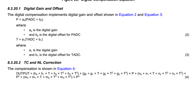
According to the thread sent by you, there should be a value stored in g0 for the output to be non-zero. This is what I infer till now:
P=a0(PADC +b0)
output=h0+g0*P
I haven't programmed any of the 4 parameters (a0, b0, h0, g0), so they must be zero but then I should get 0 as output but I do get some value at Vout.
I guess I don't have to interfere with the DAC registers additionally.
I suppose something (MCU/Compensation/IIR/Other) adds a 2.5V bias to provide for a single-ended DAC. But I guess it might invert something somewhere. What do you see if you change the (im)balance in your bridge?
I re-read Sec 8.3.18.1.2 and in my suggestion above the Address byte should probably be (0x26 >> 1). This further suggests that you must write 2 bytes at once, and writing the P_GAIN cell will also write the T_GAIN cell (0x27).
Did you try "live" updating the P_GAIN register while the device is active (not in Reset)?
I figured that in the EEPROM_PAGE_ADDRESS register, the upper 6 bits of 0x26(i.e., 0x13) are to be written. Because the EEPROM address goes from 0 to 7F (making it 7 bits max), the 0x400000 part is common to all EEPROM registers. But then my question is how will it identify whether it is 0x26 or 0x27 as 0x27 will also have 0x13 written in the EEPROM_PAGE_ADDRESS register?
In the cache registers, as given in this figure, the first byte should be the cache address and the second should be the data to be written in the register. There is no mention of a cache address in the datasheet. Maybe it will indicate whether the 0x26 or 0x27 has to be written on. But what exactly should be written in the 0x80 register of 0x45?
I think you (always) have to write 2 bytes. That would mean that writing a 1-byte setting includes writing one of the neighboring bytes as well. The neighbor would be the one that shares the 6-bit address (addr >> 1); for P_GAIN (0x26) that would be T_GAIN (0x27).
Under this interpretation, you write the two bytes into EEPROM_CACHE, the address (addr >> 1) into EEPROM_PAGE_ADDRESS, then 0x01 (Program) into EEPROM_CTRL. You could presumably write all these in a single transaction.
What isn't obvious is what byte order is expected in EEPROM_CACHE, since there are no clues in Figs 51/52. A reasonable first guess is to assume byte-order/little-endian. In that case you would write your P_GAIN (0x26) into EEPROM_CACHE[0], then a chosen T_GAIN (0x27) into EEPROM_CACHE[1].
I suggest you try it and find out. Choose a T_GAIN value that is different from what you want for P_GAIN (you've grounded the Temp input, so any T_GAIN_SEL value will do), write the values to 0x80-0x83, wait 8ms, take the device out of reset, and read the (active) values of P_GAIN and T_GAIN. If they look backwards, then you know the byte order is the other way, so reverse them in your code and write them again. (Getting it wrong costs very little.)
Thank you for the help. I was able to program the EEPROM 0x26 register and it is visible in the control register (0x47 of 0x42) as well. I plotted the PADC values with the corresponding input values, which are indeed being amplified, so the path till ADC is clear. The catch is that the amplified value can't be more than 2.5V. But I couldn't program the g0 value (it is being read as 0x00) the same way. Am I supposed to ERASE the register and then try to PROGRAM it?
The way EEPROM (usually) works is that writing a cell implicitly erases it first, so I think setting ERASE+PROGRAM really erases it to 0xFF (or maybe 0x00).
Table 10 suggests that there's no way to read the "live" (DI) copy of G0. There is the EEPROM_ARRAY[] (page 5, registers 0x00-0x7F) which is supposed to contain the EEPROM contents [Ref Table 25]. I suppose the internal MCU does the read automatically coming out of Reset, since I don't see a way to request it. Looking there might provide some confidence that your G0 write succeeded.
More generally: This thread contains a list of EEPROM settings, which I imagine were extracted (via EEPROM_ARRAY[]) from an actual chip at TI. (The first list doesn't look quite right, so use the second one.) Notably some of these values differ from what the data sheet says they should be. He also suggests that you can write the DAC output register (DAC_REG0, I guess) directly while in Reset, which might be enlightening:
Whatever I write in the G0 register reads as either 0x05 or 0x0D. This seems like a problem in other linearization coefficients as well. Also, the register description mentions that the coefficient is 2's complement, so if I want to store 0x01, do I have to write 0xFF? Even then the stored value is 0x05 or 0x0D.
On page 38, there are 2 equations for the IIR filter, I'm unable to decipher how exactly that has to be implemented. After the PADC, the value goes to digital compensation then to clamping, then to the IIR filter, and finally the DAC gain. What is the role of clamping? I wish there were a bit clearer order as to how exactly we can reach the amplified output at Vout pin 9.
How are you reading G0? Are you looking at the EEPROM value? G0 is 16 bits, have you shown all of them? That said, I don't know why you would see 0x05 after you write 0x01. The EEPROM listing in that thread I linked to shows G0=0x1000, for what that's worth.
2's complement is just normal "int" representation. +2 would be 0x0002; -2 would be 0xFFFE.
Clamping (as near as I can tell) limits the range of values that can be presented to the DAC; it might also be called "saturation". If the result is outside [NORMAL_LOW,NORMAL_HIGH] range, the CLAMP_LOW or CLAMP_HIGH value is substituted as appropriate. One thing (I suppose) this does is to keep a result of 0x4005 from being output by the DAC as though it were 0x0005. There might be other reasons for artificially reducing the output range.
Yes, I am reading the G0's EEPROM value 0x08 & 0x09 of 0x45. When I first read it without altering, it was showing 0x1000 but wouldn't that be a gain of 8? If If I keep all the clamp-related registers as 0x00, the output should be whatever comes at DAC, right?
I'm not sure what's happening with your change of G0. I haven't been through all the arithmetic; why would G0=0x1000 imply a gain of 8?
I would expect that in a fresh chip NORMAL_HIGH and CLAMP_HIGH are (both) =0x3FFF, so the value given to the DAC always fits in 14 bits. That's also what I see in the EEPROM listing in the thread I linked to. If your values are =0, then (as I understand it) the DAC value would always be =0. What values do you see there?
What do you understand by G0= 0x1000? I mostly see 4.3V at the output. But it kinda varies but not in a way that can be related to the input or gain.
In this thread, it has been mentioned that the last byte of EEPROM (7F, EEPROM_CRC) has to be programmed with a new CRC value every time a EEPROM register is modified. But the CRC value changes when the EEPROM_CRC register is modified (as it is also a eeprom register). In that case, we can never keep the same value of EEPROM_CRC_VALUE(0x86 of 0x45) in the EEPROM_CRC register. Therefore, EEPROM_CRC_STATUS always shows 0x00. What is the way out of this loop?
Sec 8.3.18.1.4 claims that the CRC is "automatically" computed and verified, so it would seem you don't need to do anything. The PGA305 data sheet (SLDS231 Sec 7.3.16.1.4) contains the same text; I don't know why that other thread seems to suggest you should compute it and store it.
I suppose EEPROM_CRC_VALUE is the result after using CALCULATE_CRC, so maybe that's what sets EEPROM_CRC_STATUS, and the automatic verification doesn't set anything.
Hey,
I programmed the EEPROM to its original settings and it worked! I was able to see the correct amplified output voltage at pin 9 for the respective gain I set. But the problems don't ever seem to end... I was earlier giving the input using a potentiometer connected to the 3.3V supply of the launchpad and it worked fine. But I have to connect this system to a setup for strain amplification, the input there is coming from a function generator and the results are not really accurate. Since my main goal is the design of strain amplifier, the input voltage levels are really low (in the range of 1 to 3mV).
The output voltage (as measured by a 6½ digit multimeter) is around 29 mV even when the input is applied to zero. So, for lower inputs, the output is this constant voltage (for P_GAIN =1.33, 2, 4). And for voltages like more than 100mV, the gain keeps decreasing. For higher gains (like 40, 100 v/v), I don't even observe any kind of amplification but just this constant voltage around 29 to 40 mV.
Firstly I thought OFFSET correction can be the issue here. But even when I set that particular register (OFFSET_CANCEL: EEPROM ADRESS=0X29), I see no significant changes in the output. It seems really strange that the circuit worked fine while using the potentiometer but has issues while using the function generator. If you have any thoughts on this, please do share.
How does the function generator fit into your system? Does it supply the bridge excitation? I have seen that many function generators can't source much current, though the data sheet test cases suggest 1mA (5V/5Kohm) is fine for the ADC.
Have you been able to read PADC_DATA (0x40/0x10-0x11)? That might help distinguish the difference between the two cases.
I'm just using the DC function generator input directly to VINPN and VINPP pins. The value of PADC_DATA and DAC code correspond to whatever output I see on the multimeter.
Is the negative of the function generator ground, or floating? Grounding one side of the bridge will unbalance it.
But does the PADC_DATA from your function generator match that for an equivalent bridge imbalance? If so, that implies (as you suggested) something in the correction.
What are the NORMAL_x and CLAMP_x values in the EEPROM?
Negative of function generator is connected VINPN which is connected to ground (pin 15)
I did not check the PADC values for input 0V but for 100mV input (gain=4).. the PADC gave the value equivalent to 114mV and DAC code also showed the same value.. but value on multimeter was 250mV.
I have now no clue what's going wrong.
The values of NORMAL_x and CLAMP_x are 0x00
The OFFSET_CANCEL register has a OFFSET_SELECT bit which determines positive or negative offset. When I set the bit(positive offset).. the offset increases but when I clear (negative offset) there is no change in the offset... It remains at least 21mV and doesn't go lower than that.
I would expect NORMAL_HIGH and CLAMP_HIGH to be =0x3FFF (as seen in that other thread). Otherwise it will (always) detect "too-high" and try to output 0, regardless of the arithmetic.
I (vaguely) recall that the DAC is not rail-to-rail, so maybe 250mV is as low as it can go.
**Attention** This is a public forum