This thread has been locked.

If you have a related question, please click the "Ask a related question" button in the top right corner. The newly created question will be automatically linked to this question.

MSP430F5359: How do I configure all four “Port J” (JTAG) pins for use as GPIOs?

Part Number: MSP430F5359
Other Parts Discussed in Thread: MSP-FET,

If I'm reading the documentation (the Data Sheet and the Family User's Guide) correctly, the four JTAG pins of the MPS430F5359 (TDO, TDI/TCLK, TMS, and TCK) can also be configured as the GPIO pins PJ.0, PJ.1, PJ.2, and PJ.3.

So I wrote some code to try to do that reconfiguration and then wiggle the pins. (You can easily guess what my various macros do.)

// SET_BITS( PJOUT, ( BIT_3 | BIT_2 | BIT_1 | BIT_0 ) );
// SET_BITS( PJDIR, ( BIT_3 | BIT_2 | BIT_1 | BIT_0 ) );

PJOUT = 0xFFFFU;
PJDIR = 0xFFFFU;

for ( uint16 i = 0; i < 10U; i++ )
{
CLR_BIT( PJOUT, BIT_0 );
DELAY_US( 10UL );

CLR_BIT( PJOUT, BIT_1 );
DELAY_US( 10UL );

CLR_BIT( PJOUT, BIT_2 );
DELAY_US( 10UL );

CLR_BIT( PJOUT, BIT_3 );
DELAY_US( 10UL );

PJOUT = 0x0000U;
DELAY_US( 10UL );

SET_BIT( PJOUT, BIT_0 );
DELAY_US( 10UL );

SET_BIT( PJOUT, BIT_1 );
DELAY_US( 10UL );

SET_BIT( PJOUT, BIT_2 );
DELAY_US( 10UL );

SET_BIT( PJOUT, BIT_3 );
DELAY_US( 10UL );

PJOUT = 0xFFFFU;
DELAY_US( 10UL );
}

But when I run this code, only TDO (PJ.0) wiggles.

The documentation states that the TEST/SBWTCK signal has some control over this but when that pin is pulled down to VSS, GPIO ought to be available; I have external logic on my board that IS pulling that pin down.

The documentation also discusses the SYSJTAGPIN bit in the SYSCTL register but the point of this is to disable GPIO use so I'm leaving that register in its default BOR state (and setting that bit DOES seem to disable my successful use of PJ.0).

Note:

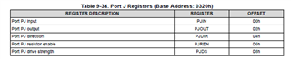
Port J doesn't have a "SEL" register to select whether the pins are GPIOs or Peripheral Function pins.

Does anyone know why I can only get PJ.0 to work as a GPIO and not PJ.1, PJ.2, or PJ.3?

  • Hi Atlant,

    Try the code below and verify it works, you dont have anything other than a scope/LA connected to the JTAG pins while you are performing this test right? 

    int main(void)
    {
      volatile unsigned int i;
    
      WDTCTL = WDTPW+WDTHOLD;                   // Stop WDT
      PJDIR |= BIT3 | BIT2 | BIT1 |BIT0;
    
      while(1)                                  // continuous loop
      {
        PJOUT ^= BIT3;
        PJOUT ^= BIT2;
        PJOUT ^= BIT1;
        PJOUT ^= BIT0;
        for(i=50000;i>0;i--);                   // Delay
      }
    }

    Best Regards,
    Brandon Fisher

  • Brandon:

    > you don't have anything other than a scope/LA connected to the JTAG pins while you are performing this test right?

    Thank you for asking this question; it broke the problem loose for me!

    The easy answer was "Yes, I'd unplugged the MSP-FET programming pod(s) that connect to our several MSP430F5359s" but in thinking about it further, I realized that on our test board, we also have SN74LVC8T245DWR "8-Bit Dual-Supply Bus Transceiver with Configurable Voltage-Level Shifting and Three-State Outputs" buffering the inward-going (from the MSP-FET to the MSP430) TDI/TCLK, TMS, and TCK signals from the 3.3V MSP-FET voltage domain to our MSP430's 2.5V voltage domain. And we'd provided pull-ups on the MSP-FET side of the level converter and hard-wired the OE (“Output Enable”) pin to ground so even when I'd unplugged the MSP-FET pods, the level converter was still driving those three signals with a pretty-stiff totem-pole high.

    (TDO, on the other hand, is routed “outward” from the MSP430 to the MSP-FET through a SN74LVC2T45DCTR level converter.)

    Looking at the three signals with an analog scope, I can definitely see that the MSP430 is trying to pull those signals low but not being able to do so against the stiff pull-up provided by the level converter.

    I didn't realize this sooner because our test fixture also has some of those magic bidirectional level-converting buffers on it and I'd forgotten that the JTAG port's level converters were unidirectional.

    So “Thanks!”, your question jogged my memory and I can now confirm that all is well with the MSP430F5359 and using its JTAG bits as GPIO ports.

    And I'll get our EEs to modify our test fixture to either automagically disable the inbound level converter when the MSP-FET is unplugged or at least to provide just a soft pull-down on the OE pin of the level converter so I can disable it when I want to use the JTAG pins as four more GPIOs.

    This question is now resolved and I thank you again for your help!

**Attention** This is a public forum