Part Number: MSP430FR59471
Tool/software:
Hi,
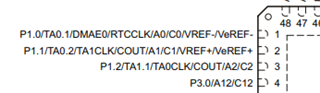
We are using the TI part MSP430FR59471IRHAT and have encountered an issue with pin 3 (P1.2/TA1.1/TAOCLK/COUT/A2/C2).
We suspect that this pin is being treated as an ADC input, which causes noise and instability in the measured analog inputs (A0, A14, and A30) when the voltage exceeds Vref INTERNAL (2.5V).
Can you help us understand how to configure this pin as an Input-GPIO in code, bypassing the 2.5V (Vref) limitation?
Here is the code we are using for pin 1.2:
P1DIR &= ~BIT2;
P1REN |= BIT2;
P1OUT &= ~BIT2;
P1IES &= ~BIT2;
P1IE |= BIT2;
Thank you for your assistance!