Tool/software:
Hi I am trying to make a bootloader compatible application my bootloader and application is working fine untill I enable 24 bit sigma delta interrupts in my code once i enable interrupts it get's into a hang state so can't make out what is happening. I am sharing my linker script and vector table file code.
following is in my linker script
.
/******************************************************************************/
/* LINKER COMMAND FILE FOR MSPBoot BOOTLOADER USING MSP430F6779A */
/* File generated with MSPBootLinkerGen.pl on 07-01-2024 */
/*----------------------------------------------------------------------------*/
/****************************************************************************/
/* SPECIFY THE SYSTEM MEMORY MAP */
/****************************************************************************/
/* The following definitions can be changed to customize the memory map for a different device
* or other adjustments
* Note that the changes should match the definitions used in MEMORY and SECTIONS
*
*/
/* RAM Memory Addresses */
__RAM_Start = 0x1C00; /* RAM Start */
__RAM_End = 0x9BFF; /* RAM End */
/* RAM shared between App and Bootloader, must be reserved */
PassWd = 0x1C00; /* Password sent by App to force boot mode */
StatCtrl = 0x1C02; /* Status and Control byte used by Comm */
CI_State_Machine = 0x1C03; /* State machine variable used by Comm */
CI_Callback_ptr = 0x1C04; /* Pointer to Comm callback structure */
/* Unreserved RAM used for Bootloader or App purposes */
_NonReserved_RAM_Start = 0x1C08; /* Non-reserved RAM */
/* Flash memory addresses */
/* App area : C000-E7FF & 10000-4CBFB*/
/* Download area: 4CBFC-8BFF7*/
/* Boot area : E800-FFFF*/
__Flash_Start = 0xC000; /* Start of Application area */
/* Reserved Flash locations for Bootloader Area */
__Boot_Start = 0xE800; /* Boot flash */
__Boot_Reset = 0xFFFE; /* Boot reset vector */
__Boot_VectorTable = 0xFF80; /* Boot vector table */
__Boot_SharedCallbacks_Len = 6; /* Length of shared callbacks (2 calls =4B(msp430) or 8B(msp430x) */
__Boot_SharedCallbacks = 0xFF7A; /* Start of Shared callbacks */
_BOOT_APPVECTOR = __Boot_SharedCallbacks; /* Definition for application table */
_Appl_Proxy_Vector_Start = 0xE702; /* Proxy interrupt table */
/* Reserved Flash locations for Application Area */
/* MEMORY definition, adjust based on definitions above */
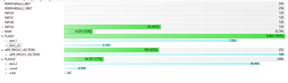
MEMORY
{
SFR : origin = 0x0000, length = 0x0010
PERIPHERALS_8BIT : origin = 0x0010, length = 0x00F0
PERIPHERALS_16BIT : origin = 0x0100, length = 0x0100
// RAM from _NonReserved_RAM_Start - __RAM_End
RAM : origin = 0x1C08, length = 0x7FF8
// Info Mem Sections
INFOA : origin = 0x1980, length = 0x80
INFOB : origin = 0x1900, length = 0x80
INFOC : origin = 0x1880, length = 0x80
INFOD : origin = 0x1800, length = 0x80
// Flash from _App_Start -> (APP_PROXY_VECTORS-1)
FLASH : origin = 0xC002, length = 0x2700
FLASH2 : origin = 0x10000, length = 0x3CBFC
// Interrupt Proxy table from _App_Proxy_Vector_Start->(RESET-1)
APP_PROXY_VECTORS : origin = 0xE702, length = 252
// App reset from _App_Reset_Vector
RESET : origin = 0xE7FE, length = 0x0002
}
/****************************************************************************/
/* SPECIFY THE SECTIONS ALLOCATION INTO MEMORY */
/****************************************************************************/
SECTIONS
{
.bss : {} > RAM /* GLOBAL & STATIC VARS */
.data : {} > RAM /* GLOBAL & STATIC VARS */
.sysmem : {} > RAM /* DYNAMIC MEMORY ALLOCATION AREA */
.stack : {} > RAM (HIGH) /* SOFTWARE SYSTEM STACK */
.text:_isr : {} > FLASH /* Code ISRs */
#ifndef __LARGE_CODE_MODEL__
.text : {} >> FLASH /* CODE */
#else
.text : {} >> FLASH | FLASH2 /* CODE */
#endif
.cinit : {} > FLASH | FLASH2 /* INITIALIZATION TABLES*/
#ifndef __LARGE_DATA_MODEL__
.const : {} >> FLASH /* CONSTANT DATA */
#else
.const : {} >> FLASH2 | FLASH /* CONSTANT DATA */
#endif
.cio : {} > RAM /* C I/O BUFFER */
.infoA : {} > INFOA /* MSP430 INFO FLASH Memory segments */
.infoB : {} > INFOB
.infoC : {} > INFOC
.infoD : {} > INFOD
.APP_PROXY_VECTORS : {} > APP_PROXY_VECTORS /* INTERRUPT PROXY TABLE */
.reset : {} > RESET /* MSP430 RESET VECTOR */
}
/****************************************************************************/
/* INCLUDE PERIPHERALS MEMORY MAP */
/****************************************************************************/
-l MSP430F6779A.cmd
the following is my 24Bit sigma delta interrupt
#if defined(__TI_COMPILER_VERSION__) || defined(__IAR_SYSTEMS_ICC__)
#pragma vector=SD24B_VECTOR
__interrupt void SD24BISR(void) {
#elif defined(__GNUC__)
void __attribute__ ((interrupt(SD24_VECTOR))) SD24_ISR(void)
#else
#error Compiler not supported!
#endif
    int16_t tempV;
    int32_t tempI;
    switch(SD24BIV)
    {
    case SD24BIV_SD24IFG0:                  // SD24MEM0 IFG
        chReadStatus |= HAL_ADC_CH0_READ;

        // Store Voltage Results
        phAVSamples[phAWriteVIdx] = SD24_B_getHighWordResults(SD24_BASE, SD24_B_CONVERTER_0);

        // Apply Voltage DC Filter
        tempV = EM_voltageDCFilter(&gEmSWResult.phaseBGResults[EM_PH_A_IDX].vDCEstimate, phAVSamples[phAWriteVIdx]);
        phAVSamples[phAWriteVIdx] = tempV;

        // Increase Index and Mask
        phAWriteVIdx = (phAWriteVIdx+1) & (HAL_ADC_V_MASK);
        break;
    case SD24BIV_SD24IFG1:                  // SD24MEM1 IFG
        chReadStatus |= HAL_ADC_CH1_READ;

        // Store Voltage Results
        phBVSamples[phBWriteVIdx] = SD24_B_getHighWordResults(SD24_BASE, SD24_B_CONVERTER_1);

        // Apply Voltage DC Filter
        tempV = EM_voltageDCFilter(&gEmSWResult.phaseBGResults[EM_PH_B_IDX].vDCEstimate, phBVSamples[phBWriteVIdx]);
        phBVSamples[phBWriteVIdx] = tempV;

        // Increase Index and Mask
        phBWriteVIdx = (phBWriteVIdx+1) & (HAL_ADC_V_MASK);
        break;
    case SD24BIV_SD24IFG2:                  // SD24MEM2 IFG
        chReadStatus |= HAL_ADC_CH2_READ;

        // Store Voltage Results
        phCVSamples[phCWriteVIdx] = SD24_B_getHighWordResults(SD24_BASE, SD24_B_CONVERTER_2);

        // Apply Voltage DC Filter
        tempV = EM_voltageDCFilter(&gEmSWResult.phaseBGResults[EM_PH_C_IDX].vDCEstimate, phCVSamples[phCWriteVIdx]);
        phCVSamples[phCWriteVIdx] = tempV;

        // Increase Index and Mask
        phCWriteVIdx = (phCWriteVIdx+1) & (HAL_ADC_V_MASK);
        break;
    case SD24BIV_SD24IFG3:                  // SD24MEM3 IFG
        break;
    case SD24BIV_SD24IFG4:                  // SD24MEM4 IFG
        chReadStatus |= HAL_ADC_CH4_READ;

        // Store Current Results
        phAISamples[phAWriteIIdx] = SD24_B_getResults(SD24_BASE, SD24_B_CONVERTER_4);
        tempI = phAISamples[phAWriteIIdx] >> 1;
        phAISamples[phAWriteIIdx] = tempI;

        // Apply Current DC Filter
        tempI = EM_currentDCFilter(gEmSWResult.phaseBGResults[EM_PH_A_IDX].iDCEstimate, phAISamples[phAWriteIIdx]);
        phAISamples[phAWriteIIdx] = tempI;

        // Increase Index and Mask
        phAWriteIIdx = (phAWriteIIdx+1) & (HAL_ADC_I_MASK);
        break;
    case SD24BIV_SD24IFG5:                  // SD24MEM5 IFG
        chReadStatus |= HAL_ADC_CH5_READ;

        // Store Current Results
        phBISamples[phBWriteIIdx] = SD24_B_getResults(SD24_BASE, SD24_B_CONVERTER_5);
        tempI = phBISamples[phBWriteIIdx] >> 1;
        phBISamples[phBWriteIIdx] = tempI;

        // Apply Current DC Filter
        tempI = EM_currentDCFilter(gEmSWResult.phaseBGResults[EM_PH_B_IDX].iDCEstimate, phBISamples[phBWriteIIdx]);
        phBISamples[phBWriteIIdx] = tempI;

        // Increase Index and Mask
        phBWriteIIdx = (phBWriteIIdx+1) & (HAL_ADC_I_MASK);
        break;
    case SD24BIV_SD24IFG6:                  // SD24MEM6 IFG
        chReadStatus |= HAL_ADC_CH6_READ;

        // Store Current Results
        phCISamples[phCWriteIIdx] = SD24_B_getResults(SD24_BASE, SD24_B_CONVERTER_6);
        tempI = phCISamples[phCWriteIIdx] >> 1;
        phCISamples[phCWriteIIdx] = tempI;

        // Apply Current DC Filter
        tempI = EM_currentDCFilter(gEmSWResult.phaseBGResults[EM_PH_C_IDX].iDCEstimate, phCISamples[phCWriteIIdx]);
        phCISamples[phCWriteIIdx] = tempI;

        // Increase Index and Mask
        phCWriteIIdx = (phCWriteIIdx+1) & (HAL_ADC_I_MASK);
        break;
    default: break;
    }

    // Check if both channels were read for all phases
    if((chReadStatus & (HAL_ADC_CH0_READ+HAL_ADC_CH1_READ+HAL_ADC_CH2_READ+HAL_ADC_CH4_READ+HAL_ADC_CH5_READ+HAL_ADC_CH6_READ)) ==
       (HAL_ADC_CH0_READ+HAL_ADC_CH1_READ+HAL_ADC_CH2_READ+HAL_ADC_CH4_READ+HAL_ADC_CH5_READ+HAL_ADC_CH6_READ))
    {
        chReadStatus = 0;

        // Pulse Generation for Total Energy
        if(phASA == 0 || phBSA == 0 || phCSA == 0)
        {
            // Check Energy and Generate Pulses
            EM_genPulseTotalPhases(gEmSWConfig.systemConfig,
                                     &gEmSWConfig.systemConfig->pulseArray[EM_PH_TOTAL_IDX],
                                     gEmSWResult.emTotalResult);
        }
        // Phase A Data Processing
        if(phASA == 0)
        {
            // Voltage aligned with Current
            if(phAProc == 0)
            {
                phAProc = 1;
            }
            else
            {
                // Increase Current (I) Index and Mask
                phAIIdx = (phAIIdx+1) & HAL_ADC_I_MASK;

                // Increase Voltage (V) Index and Mask
                phAVIdx = (phAVIdx+1) & HAL_ADC_V_MASK;
            }

            // Set the Ptrs to voltage and current
            emPhaseConfiguration[EM_PH_A_IDX].voltageSamplePtr = &phAVSamples[phAVIdx];
            emPhaseConfiguration[EM_PH_A_IDX].currentSamplePtr = &phAISamples[phAIIdx];

            // Process the samples
            EM_perSampleProc(gEmSWResult.phaseMetrologyPing[EM_PH_A_IDX],
                             &gEmSWConfig.meterConfig->phaseConfigPtr[EM_PH_A_IDX],
                             &gEmSWResult.phaseBGResults[EM_PH_A_IDX]);

            // Check Energy and Generate Pulses
            EM_genPulseIndPhase(gEmSWConfig.systemConfig,
                                &gEmSWConfig.systemConfig->pulseArray[EM_PH_A_IDX],
                                &gEmSWResult.phaseResults[EM_PH_A_IDX]);

            if(gEmSWResult.phaseMetrologyPing[EM_PH_A_IDX]->cycleCount == gEmSWConfig.algorithmConfig->mainNomFreq)
            {
                phaseDataReady |= HAL_ADC_PHASE_A_DATA_READY;
                EM_perDataChunk(&gEmSWConfig, (EM_SW_Lib_Result_Handle *) &gEmSWResult, EM_PH_A_IDX);
            }
            else if (gEmSWResult.phaseMetrologyPing[EM_PH_A_IDX]->sampleCount > (2*EM_SAMPLING_FREQ_HZ))
            {
                phaseDataReady |= HAL_ADC_PHASE_A_DATA_READY;
                EM_perDataChunk(&gEmSWConfig, (EM_SW_Lib_Result_Handle *) &gEmSWResult, EM_PH_A_IDX);
            }
        }
        else if(phASA > 0)
        {
            // Voltage leading Current
            phASA = phASA-1;
            phAIIdx = phAIIdx+1;
        }
        else
        {
            // Voltage lagging Current
            phASA = phASA+1;
            phAVIdx = phAVIdx+1;
        }
        // Phase B Data Processing
        if(phBSA == 0)
        {
            // Voltage aligned with Current
            if(phBProc == 0)
            {
                phBProc = 1;
            }
            else
            {
                // Increase Current (I) Index and Mask
                phBIIdx = (phBIIdx+1) & HAL_ADC_I_MASK;

                // Increase Voltage (V) Index and Mask
                phBVIdx = (phBVIdx+1) & HAL_ADC_V_MASK;
            }

            // Set the Ptrs to voltage and current
            emPhaseConfiguration[EM_PH_B_IDX].voltageSamplePtr = &phBVSamples[phBVIdx];
            emPhaseConfiguration[EM_PH_B_IDX].currentSamplePtr = &phBISamples[phBIIdx];

            // Process the samples
            EM_perSampleProc(gEmSWResult.phaseMetrologyPing[EM_PH_B_IDX],
                             &gEmSWConfig.meterConfig->phaseConfigPtr[EM_PH_B_IDX],
                             &gEmSWResult.phaseBGResults[EM_PH_B_IDX]);

            // Check Energy and Generate Pulses
            EM_genPulseIndPhase(gEmSWConfig.systemConfig,
                                &gEmSWConfig.systemConfig->pulseArray[EM_PH_B_IDX],
                                &gEmSWResult.phaseResults[EM_PH_B_IDX]);

            if(gEmSWResult.phaseMetrologyPing[EM_PH_B_IDX]->cycleCount == gEmSWConfig.algorithmConfig->mainNomFreq)
            {
                phaseDataReady |= HAL_ADC_PHASE_B_DATA_READY;
                EM_perDataChunk(&gEmSWConfig, (EM_SW_Lib_Result_Handle *) &gEmSWResult, EM_PH_B_IDX);
            }
            else if (gEmSWResult.phaseMetrologyPing[EM_PH_B_IDX]->sampleCount > (2*EM_SAMPLING_FREQ_HZ))
            {
                phaseDataReady |= HAL_ADC_PHASE_B_DATA_READY;
                EM_perDataChunk(&gEmSWConfig, (EM_SW_Lib_Result_Handle *) &gEmSWResult, EM_PH_B_IDX);
            }
        }
        else if(phBSA > 0)
        {
            // Voltage leading Current
            phBSA = phBSA-1;
            phBIIdx = phBIIdx+1;
        }
        else
        {
            // Voltage lagging Current
            phBSA = phBSA+1;
            phBVIdx = phBVIdx+1;
        }
        // Phase C Data Processing
        if(phCSA == 0)
        {
            // Voltage aligned with Current
            if(phCProc == 0)
            {
                phCProc = 1;
            }
            else
            {
                // Increase Current (I) Index and Mask
                phCIIdx = (phCIIdx+1) & HAL_ADC_I_MASK;

                // Increase Voltage (V) Index and Mask
                phCVIdx = (phCVIdx+1) & HAL_ADC_V_MASK;
            }

            // Set the Ptrs to voltage and current
            emPhaseConfiguration[EM_PH_C_IDX].voltageSamplePtr = &phCVSamples[phCVIdx];
            emPhaseConfiguration[EM_PH_C_IDX].currentSamplePtr = &phCISamples[phCIIdx];

            // Process the samples
            EM_perSampleProc(gEmSWResult.phaseMetrologyPing[EM_PH_C_IDX],
                             &gEmSWConfig.meterConfig->phaseConfigPtr[EM_PH_C_IDX],
                             &gEmSWResult.phaseBGResults[EM_PH_C_IDX]);

            // Check Energy and Generate Pulses
            EM_genPulseIndPhase(gEmSWConfig.systemConfig,
                                &gEmSWConfig.systemConfig->pulseArray[EM_PH_C_IDX],
                                &gEmSWResult.phaseResults[EM_PH_C_IDX]);

            if(gEmSWResult.phaseMetrologyPing[EM_PH_C_IDX]->cycleCount == gEmSWConfig.algorithmConfig->mainNomFreq)
            {
                phaseDataReady |= HAL_ADC_PHASE_C_DATA_READY;
                EM_perDataChunk(&gEmSWConfig, (EM_SW_Lib_Result_Handle *) &gEmSWResult, EM_PH_C_IDX);
            }
            else if (gEmSWResult.phaseMetrologyPing[EM_PH_C_IDX]->sampleCount > (2*EM_SAMPLING_FREQ_HZ))
            {
                phaseDataReady |= HAL_ADC_PHASE_C_DATA_READY;
                EM_perDataChunk(&gEmSWConfig, (EM_SW_Lib_Result_Handle *) &gEmSWResult, EM_PH_C_IDX);
            }
        }
        else if(phCSA > 0)
        {
            // Voltage leading Current
            phCSA = phCSA-1;
            phCIIdx = phCIIdx+1;
        }
        else
        {
            // Voltage lagging Current
            phCSA = phCSA+1;
            phCVIdx = phCVIdx+1;
        }
    }
}
the following is how my vector table is defined in file TI_MSPBoot_Mgr_Vectors_F6779A.c which was generated using MSPBoot
/******************************************************************************/
/* Vector Redirection FILE FOR MSPBoot Application USING MSP430F6779A */
/* File generated with MSPBootVecRedGen.pl on 07-01-2024 */
/*----------------------------------------------------------------------------*/
#include "msp430.h"
#include <stdint.h>
#include "TI_MSPBoot_Mgr_Vectors.h"
// Global variables
/*! Password sent by Application to force boot mode. This variable is in a fixed
location and should keep same functionality and location in Boot and App */
extern uint16_t PassWd;
/*! Status and Control byte. This variable is in a fixed
location and should keep same functionality and location in Boot and App */
extern uint8_t StatCtrl;
/******************************************************************************
*
* @brief Forces Boot mode
* Sets a bit in Status and Control byte to request Boot mode, writes a password
* in PassWd and forces a PUC reset
* Boot will start execution after PUC and detect forced Boot mode
*
* @return none
*****************************************************************************/
void TI_MSPBoot_JumpToBoot( void )
{
PassWd = BSL_PASSWORD; // Send password
StatCtrl |= BOOT_APP_REQ; // Set flag to request boot mode
__disable_interrupt(); // Disable all interrupts
WDTCTL = WDT_MRST_0_064; // Set watchdog and wait for expiration
while (1);
}
//
// External ISR prototypes used by ProxyVectorTable
// Add your own ISRs as shown below
//
//TODO: Add extern prototypes of every ISR in your system
extern __interrupt void Dummy_Isr (void);
extern __interrupt void RTC_ISR (void);
extern __interrupt void PORT1_ISR (void);
extern __interrupt void PORT2_ISR (void);
extern __interrupt void DMA_ISR (void);
extern __interrupt void TIMER0_A0_ISR (void);
extern __interrupt void USCI_A2_ISR (void);
extern __interrupt void USCI_B1_ISR (void);
extern __interrupt void UART_ISR (void);
extern __interrupt void WDT_ISR (void);
extern __interrupt void UNMI_ISR (void);
extern __interrupt void SD24BISR (void);
#ifdef SHARED_PI
extern __interrupt void TI_MSPBoot_Comm_Isr(void);
#endif
//
// Constant tables
//
/*! This is a "proxy" interrupt table which is used by the bootloader to jump to
each interrupt routine.
It always resides in the same location.
It contains a BRA instruction (0x4030) followed by the address of each
vector routine.
Unimplemented vectors are removed (and unused vectors can be removed too)
to save flash space
*/
////TODO: Update with the interrupt vectors used in your application, see examples
//#pragma DATA_SECTION(ProxyVectorTable, ".APP_PROXY_VECTORS")
//#pragma RETAIN(ProxyVectorTable)
//const uint16_t ProxyVectorTable[] =
//{
// 0x4030, (uint16_t) DUMMY_ISR, // APP_PROXY_VECTOR(0) AES
// 0x4030, (uint16_t) DUMMY_ISR, // APP_PROXY_VECTOR(1) COMP_B
// 0x4030, (uint16_t) RTC_ISR, // APP_PROXY_VECTOR(2) RTC
// 0x4030, (uint16_t) DUMMY_ISR, // APP_PROXY_VECTOR(3) LCD_C
// 0x4030, (uint16_t) DUMMY_ISR, // APP_PROXY_VECTOR(4) TIMER3_A1
// 0x4030, (uint16_t) DUMMY_ISR, // APP_PROXY_VECTOR(5) TIMER3_A0
// 0x4030, (uint16_t) PORT2_ISR, // APP_PROXY_VECTOR(6) PORT2
// 0x4030, (uint16_t) DUMMY_ISR, // APP_PROXY_VECTOR(7) TIMER2_A1
// 0x4030, (uint16_t) DUMMY_ISR, // APP_PROXY_VECTOR(8) TIMER2_A0
// 0x4030, (uint16_t) PORT1_ISR, // APP_PROXY_VECTOR(9) PORT1
// 0x4030, (uint16_t) USCI_B1_ISR, // APP_PROXY_VECTOR(10) USCI_B1
// 0x4030, (uint16_t) DUMMY_ISR, // APP_PROXY_VECTOR(11) USCI_A3
// 0x4030, (uint16_t) DUMMY_ISR, // APP_PROXY_VECTOR(12) TIMER1_A1
// 0x4030, (uint16_t) DUMMY_ISR, // APP_PROXY_VECTOR(13) TIMER1_A0
// 0x4030, (uint16_t) DMA_ISR, // APP_PROXY_VECTOR(14) DMA
// 0x4030, (uint16_t) DUMMY_ISR, // APP_PROXY_VECTOR(15) AUX
// 0x4030, (uint16_t) USCI_A2_ISR, // APP_PROXY_VECTOR(16) USCI_A2
// 0x4030, (uint16_t) DUMMY_ISR, // APP_PROXY_VECTOR(17) USCI_A1
// 0x4030, (uint16_t) DUMMY_ISR, // APP_PROXY_VECTOR(18) TIMER0_A1
// 0x4030, (uint16_t) TIMER0_A0_ISR, // APP_PROXY_VECTOR(19) TIMER0_A0
// 0x4030, (uint16_t) SD24BISR, // APP_PROXY_VECTOR(20) SD24B
// 0x4030, (uint16_t) DUMMY_ISR, // APP_PROXY_VECTOR(21) ADC10
// 0x4030, (uint16_t) DUMMY_ISR, // APP_PROXY_VECTOR(22) USCI_B0
// 0x4030, (uint16_t) UART_ISR, // APP_PROXY_VECTOR(23) USCI_A0
// 0x4030, (uint16_t) WDT_ISR, // APP_PROXY_VECTOR(24) WDT
// 0x4030, (uint16_t) UNMI_ISR, // APP_PROXY_VECTOR(25) UNMI
// 0x4030, (uint16_t) DUMMY_ISR, // APP_PROXY_VECTOR(26) SYSNMI
//};
//TODO: Update with the interrupt vectors used in your application, see examples
#pragma DATA_SECTION(ProxyVectorTable, ".APP_PROXY_VECTORS")
#pragma RETAIN(ProxyVectorTable)
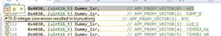
const uint16_t ProxyVectorTable[] =
{
0x4030, (uint16_t) Dummy_Isr, // APP_PROXY_VECTOR(0) AES
0x4030, (uint16_t) Dummy_Isr, // APP_PROXY_VECTOR(1) COMP_B
0x4030, (uint16_t) RTC_ISR, // APP_PROXY_VECTOR(2) RTC
0x4030, (uint16_t) Dummy_Isr, // APP_PROXY_VECTOR(3) LCD_C
0x4030, (uint16_t) Dummy_Isr, // APP_PROXY_VECTOR(4) TIMER3_A1
0x4030, (uint16_t) Dummy_Isr, // APP_PROXY_VECTOR(5) TIMER3_A0
0x4030, (uint16_t) PORT2_ISR, // APP_PROXY_VECTOR(6) PORT2
0x4030, (uint16_t) Dummy_Isr, // APP_PROXY_VECTOR(7) TIMER2_A1
0x4030, (uint16_t) Dummy_Isr, // APP_PROXY_VECTOR(8) TIMER2_A0
0x4030, (uint16_t) PORT1_ISR, // APP_PROXY_VECTOR(9) PORT1
0x4030, (uint16_t) USCI_B1_ISR, // APP_PROXY_VECTOR(10) USCI_B1
0x4030, (uint16_t) Dummy_Isr, // APP_PROXY_VECTOR(11) USCI_A3
0x4030, (uint16_t) Dummy_Isr, // APP_PROXY_VECTOR(12) TIMER1_A1
0x4030, (uint16_t) Dummy_Isr, // APP_PROXY_VECTOR(13) TIMER1_A0
0x4030, (uint16_t) DMA_ISR, // APP_PROXY_VECTOR(14) DMA
0x4030, (uint16_t) Dummy_Isr, // APP_PROXY_VECTOR(15) AUX
0x4030, (uint16_t) USCI_A2_ISR, // APP_PROXY_VECTOR(16) USCI_A2
0x4030, (uint16_t) Dummy_Isr, // APP_PROXY_VECTOR(17) USCI_A1
0x4030, (uint16_t) Dummy_Isr, // APP_PROXY_VECTOR(18) TIMER0_A1
0x4030, (uint16_t) TIMER0_A0_ISR, // APP_PROXY_VECTOR(19) TIMER0_A0
0x4030, (uint16_t) SD24BISR, // APP_PROXY_VECTOR(20) SD24B
0x4030, (uint16_t) Dummy_Isr, // APP_PROXY_VECTOR(21) ADC10
0x4030, (uint16_t) Dummy_Isr, // APP_PROXY_VECTOR(22) USCI_B0
0x4030, (uint16_t) UART_ISR, // APP_PROXY_VECTOR(23) USCI_A0
0x4030, (uint16_t) WDT_ISR, // APP_PROXY_VECTOR(24) WDT
0x4030, (uint16_t) UNMI_ISR, // APP_PROXY_VECTOR(25) UNMI
0x4030, (uint16_t) Dummy_Isr, // APP_PROXY_VECTOR(26) SYSNMI
};
I am also getting the below given warning in this file