- Ask a related questionWhat is a related question?A related question is a question created from another question. When the related question is created, it will be automatically linked to the original question.
Tool/software:
Dear expert,
My customer is using MSP-GANG as programming tool for LP-MSPM0G3507.
they faced the issue when programming, see the status below.
But they are able to program MCU with XDS110, so the MCU works well.
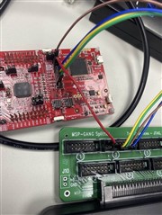
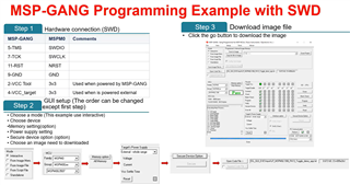
This is the way they connect the board, follow the way from our SOP.
But they can program anything into MCU.
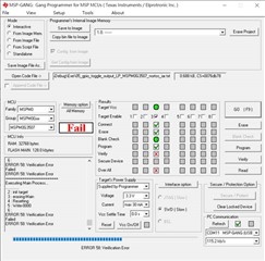
Do you know anything we have to take a look on?
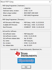
The self test report is also fine. See this.
=== MSP-GANG Self test results ( Wednesday, November 27, 2024,  11:38:25 ) ===

Adapter SN ------:  17080743
Hardware --------:  G430:  01.04
Access key ------:  MSP-GANG Programmer
Silicon Number --:  8DC0 B06F 2300 0A00
API Firmware ----:  MSP-Gang   A430:  01.03.09.00
BOOT Firmware ---:  G430BOOT   B430:  01.00.02.00
GUI Software ----:  MSP-Gang-GUI   G430:  01.03.09.00
DLL Software ----:  MSP-Gang-DLL   D430:  01.03.09.00

================ Test results =============


No.       name                   parameter       limits               result         status


  1: Data Bus   (ALL LOW)          0x0000   (0x0000  - 0x0000)  Result:  0x00     ... >>  OK   <<
  2: Data Bus   (ALL HIGH)         0x00FF   (0xFFFF  - 0xFFFF)  Result:  0xFFFF   ... >>  OK   <<
  3: Data Bus   (D-0 HI )          0x0001   (0x0101  - 0x0101)  Result:  0x0101   ... >>  OK   <<
  4: Data Bus   (D-1 HI )          0x0002   (0x0202  - 0x0202)  Result:  0x0202   ... >>  OK   <<
  5: Data Bus   (D-2 HI )          0x0004   (0x0404  - 0x0404)  Result:  0x0404   ... >>  OK   <<
  6: Data Bus   (D-3 HI )          0x0008   (0x0808  - 0x0808)  Result:  0x0808   ... >>  OK   <<
  7: Data Bus   (D-4 HI )          0x0010   (0x1010  - 0x1010)  Result:  0x1010   ... >>  OK   <<
  8: Data Bus   (D-5 HI )          0x0020   (0x2020  - 0x2020)  Result:  0x2020   ... >>  OK   <<
  9: Data Bus   (D-6 HI )          0x0040   (0x4040  - 0x4040)  Result:  0x4040   ... >>  OK   <<
 10: Data Bus   (D-7 HI )          0x0080   (0x8080  - 0x8080)  Result:  0x8080   ... >>  OK   <<

 11: Data-2 Bus  (ALL LOW)         0x0000   (0x0000  - 0x0000)  Result:  0x00     ... >>  OK   <<
 12: Data-2 Bus  (ALL HIGH)        0x00FF   (0xFFFF  - 0xFFFF)  Result:  0xFFFF   ... >>  OK   <<
 13: Data-2 Bus  (D2-0 HI )        0x0001   (0x0101  - 0x0101)  Result:  0x0101   ... >>  OK   <<
 14: Data-2 Bus  (D2-1 HI )        0x0002   (0x0202  - 0x0202)  Result:  0x0202   ... >>  OK   <<
 15: Data-2 Bus  (D2-2 HI )        0x0004   (0x0404  - 0x0404)  Result:  0x0404   ... >>  OK   <<
 16: Data-2 Bus  (D2-3 HI )        0x0008   (0x0808  - 0x0808)  Result:  0x0808   ... >>  OK   <<
 17: Data-2 Bus  (D2-4 HI )        0x0010   (0x1010  - 0x1010)  Result:  0x1010   ... >>  OK   <<
 18: Data-2 Bus  (D2-5 HI )        0x0020   (0x2020  - 0x2020)  Result:  0x2020   ... >>  OK   <<
 19: Data-2 Bus  (D2-6 HI )        0x0040   (0x4040  - 0x4040)  Result:  0x4040   ... >>  OK   <<
 20: Data-2 Bus  (D2-7 HI )        0x0080   (0x8080  - 0x8080)  Result:  0x8080   ... >>  OK   <<

 21: Vcc Target-1 (ALL OFF)         0.00 V  (  0.00 to   0.30)  Result:  0.02 V   ... >>  OK   <<
 22: Vcc Target-2 (ALL OFF)         0.00 V  (  0.00 to   0.30)  Result:  0.01 V   ... >>  OK   <<
 23: Vcc Target-3 (ALL OFF)         0.00 V  (  0.00 to   0.30)  Result:  0.01 V   ... >>  OK   <<
 24: Vcc Target-4 (ALL OFF)         0.00 V  (  0.00 to   0.30)  Result:  0.01 V   ... >>  OK   <<
 25: Vcc Target-5 (ALL OFF)         0.00 V  (  0.00 to   0.30)  Result:  0.01 V   ... >>  OK   <<
 26: Vcc Target-6 (ALL OFF)         0.00 V  (  0.00 to   0.30)  Result:  0.01 V   ... >>  OK   <<
 27: Vcc Target-7 (ALL OFF)         0.00 V  (  0.00 to   0.30)  Result:  0.01 V   ... >>  OK   <<
 28: Vcc Target-8 (ALL OFF)         0.00 V  (  0.00 to   0.30)  Result:  0.01 V   ... >>  OK   <<

 29: Translators VT (OFF)           0.00 V  (  0.00 to   0.50)  Result:  0.01 V   ... >>  OK   <<
 30: Translators VT (ON 1.8V)       1.80 V  (  1.60 to   2.00)  Result:  1.77 V   ... >>  OK   <<
 31: Translators VT (ON 2.7V)       2.70 V  (  2.50 to   2.90)  Result:  2.68 V   ... >>  OK   <<
 32: Translators VT (ON 3.6V)       3.60 V  (  3.40 to   3.80)  Result:  3.58 V   ... >>  OK   <<

 33: Vpp Voltage-in                10.00 V  (  8.00 to  12.00)  Result:  9.99 V   ... >>  OK   <<
 34: Vpp Voltage                    7.00 V  (  6.50 to   7.30)  Result:  6.88 V   ... >>  OK   <<
 35: Internal Vcc-3.3V              3.30 V  (  3.20 to   3.40)  Result:  3.31 V   ... >>  OK   <<

 36: Vcc Target-1 (ALL ON 1.8V)     1.80 V  (  1.60 to   2.00)  Result:  1.80 V   ... >>  OK   <<
 37: Vcc Target-2 (ALL ON 1.8V)     1.80 V  (  1.60 to   2.00)  Result:  1.81 V   ... >>  OK   <<
 38: Vcc Target-3 (ALL ON 1.8V)     1.80 V  (  1.60 to   2.00)  Result:  1.82 V   ... >>  OK   <<
 39: Vcc Target-4 (ALL ON 1.8V)     1.80 V  (  1.60 to   2.00)  Result:  1.81 V   ... >>  OK   <<
 40: Vcc Target-5 (ALL ON 1.8V)     1.80 V  (  1.60 to   2.00)  Result:  1.80 V   ... >>  OK   <<
 41: Vcc Target-6 (ALL ON 1.8V)     1.80 V  (  1.60 to   2.00)  Result:  1.79 V   ... >>  OK   <<
 42: Vcc Target-7 (ALL ON 1.8V)     1.80 V  (  1.60 to   2.00)  Result:  1.80 V   ... >>  OK   <<
 43: Vcc Target-8 (ALL ON 1.8V)     1.80 V  (  1.60 to   2.00)  Result:  1.80 V   ... >>  OK   <<
 44: Vcc Target-1 (ALL ON 2.7V)     2.70 V  (  2.50 to   2.90)  Result:  2.69 V   ... >>  OK   <<
 45: Vcc Target-2 (ALL ON 2.7V)     2.70 V  (  2.50 to   2.90)  Result:  2.70 V   ... >>  OK   <<
 46: Vcc Target-3 (ALL ON 2.7V)     2.70 V  (  2.50 to   2.90)  Result:  2.72 V   ... >>  OK   <<
 47: Vcc Target-4 (ALL ON 2.7V)     2.70 V  (  2.50 to   2.90)  Result:  2.72 V   ... >>  OK   <<
 48: Vcc Target-5 (ALL ON 2.7V)     2.70 V  (  2.50 to   2.90)  Result:  2.69 V   ... >>  OK   <<
 49: Vcc Target-6 (ALL ON 2.7V)     2.70 V  (  2.50 to   2.90)  Result:  2.69 V   ... >>  OK   <<
 50: Vcc Target-7 (ALL ON 2.7V)     2.70 V  (  2.50 to   2.90)  Result:  2.70 V   ... >>  OK   <<
 51: Vcc Target-8 (ALL ON 2.7V)     2.70 V  (  2.50 to   2.90)  Result:  2.70 V   ... >>  OK   <<
 52: Vcc Target-1 (ALL ON 3.6V)     3.60 V  (  3.40 to   3.80)  Result:  3.58 V   ... >>  OK   <<
 53: Vcc Target-2 (ALL ON 3.6V)     3.60 V  (  3.40 to   3.80)  Result:  3.59 V   ... >>  OK   <<
 54: Vcc Target-3 (ALL ON 3.6V)     3.60 V  (  3.40 to   3.80)  Result:  3.62 V   ... >>  OK   <<
 55: Vcc Target-4 (ALL ON 3.6V)     3.60 V  (  3.40 to   3.80)  Result:  3.62 V   ... >>  OK   <<
 56: Vcc Target-5 (ALL ON 3.6V)     3.60 V  (  3.40 to   3.80)  Result:  3.60 V   ... >>  OK   <<
 57: Vcc Target-6 (ALL ON 3.6V)     3.60 V  (  3.40 to   3.80)  Result:  3.59 V   ... >>  OK   <<
 58: Vcc Target-7 (ALL ON 3.6V)     3.60 V  (  3.40 to   3.80)  Result:  3.61 V   ... >>  OK   <<
 59: Vcc Target-8 (ALL ON 3.6V)     3.60 V  (  3.40 to   3.80)  Result:  3.60 V   ... >>  OK   <<

 60: Vcc discharge (100ms)Target-1  3.60 V  (  1.00 to   2.70)  Result:  1.09 V   ... >>  OK   <<
 61: Vcc discharge (100ms)Target-2  3.60 V  (  1.00 to   2.70)  Result:  1.11 V   ... >>  OK   <<
 62: Vcc discharge (100ms)Target-3  3.60 V  (  1.00 to   2.70)  Result:  1.10 V   ... >>  OK   <<
 63: Vcc discharge (100ms)Target-4  3.60 V  (  1.00 to   2.70)  Result:  1.10 V   ... >>  OK   <<
 64: Vcc discharge (100ms)Target-5  3.60 V  (  1.00 to   2.70)  Result:  1.12 V   ... >>  OK   <<
 65: Vcc discharge (100ms)Target-6  3.60 V  (  1.00 to   2.70)  Result:  1.11 V   ... >>  OK   <<
 66: Vcc discharge (100ms)Target-7  3.60 V  (  1.00 to   2.70)  Result:  1.09 V   ... >>  OK   <<
 67: Vcc discharge (100ms)Target-8  3.60 V  (  1.00 to   2.70)  Result:  1.12 V   ... >>  OK   <<

 68: Vcc Target-1 ( #1 ON )         0.00 V  (  3.10 to   3.50)  Result:  3.29 V   ... >>  OK   <<
 69: Vcc Target-2 ( #1 ON )         0.00 V  (  0.00 to   0.50)  Result:  0.15 V   ... >>  OK   <<
 70: Vcc Target-3 ( #1 ON )         0.00 V  (  0.00 to   0.50)  Result:  0.15 V   ... >>  OK   <<
 71: Vcc Target-4 ( #1 ON )         0.00 V  (  0.00 to   0.50)  Result:  0.15 V   ... >>  OK   <<
 72: Vcc Target-5 ( #1 ON )         0.00 V  (  0.00 to   0.50)  Result:  0.15 V   ... >>  OK   <<
 73: Vcc Target-6 ( #1 ON )         0.00 V  (  0.00 to   0.50)  Result:  0.14 V   ... >>  OK   <<
 74: Vcc Target-7 ( #1 ON )         0.00 V  (  0.00 to   0.50)  Result:  0.15 V   ... >>  OK   <<
 75: Vcc Target-8 ( #1 ON )         3.30 V  (  0.00 to   0.50)  Result:  0.14 V   ... >>  OK   <<
 76: Vcc Target-1 ( #2 ON )         0.00 V  (  0.00 to   0.50)  Result:  0.15 V   ... >>  OK   <<
 77: Vcc Target-2 ( #2 ON )         0.00 V  (  3.10 to   3.50)  Result:  3.29 V   ... >>  OK   <<
 78: Vcc Target-3 ( #2 ON )         0.00 V  (  0.00 to   0.50)  Result:  0.15 V   ... >>  OK   <<
 79: Vcc Target-4 ( #2 ON )         0.00 V  (  0.00 to   0.50)  Result:  0.15 V   ... >>  OK   <<
 80: Vcc Target-5 ( #2 ON )         0.00 V  (  0.00 to   0.50)  Result:  0.15 V   ... >>  OK   <<
 81: Vcc Target-6 ( #2 ON )         0.00 V  (  0.00 to   0.50)  Result:  0.14 V   ... >>  OK   <<
 82: Vcc Target-7 ( #2 ON )         0.00 V  (  0.00 to   0.50)  Result:  0.15 V   ... >>  OK   <<
 83: Vcc Target-8 ( #2 ON )         3.30 V  (  0.00 to   0.50)  Result:  0.14 V   ... >>  OK   <<
 84: Vcc Target-1 ( #3 ON )         0.00 V  (  0.00 to   0.50)  Result:  0.15 V   ... >>  OK   <<
 85: Vcc Target-2 ( #3 ON )         0.00 V  (  0.00 to   0.50)  Result:  0.15 V   ... >>  OK   <<
 86: Vcc Target-3 ( #3 ON )         0.00 V  (  3.10 to   3.50)  Result:  3.31 V   ... >>  OK   <<
 87: Vcc Target-4 ( #3 ON )         0.00 V  (  0.00 to   0.50)  Result:  0.15 V   ... >>  OK   <<
 88: Vcc Target-5 ( #3 ON )         0.00 V  (  0.00 to   0.50)  Result:  0.15 V   ... >>  OK   <<
 89: Vcc Target-6 ( #3 ON )         0.00 V  (  0.00 to   0.50)  Result:  0.14 V   ... >>  OK   <<
 90: Vcc Target-7 ( #3 ON )         0.00 V  (  0.00 to   0.50)  Result:  0.15 V   ... >>  OK   <<
 91: Vcc Target-8 ( #3 ON )         3.30 V  (  0.00 to   0.50)  Result:  0.14 V   ... >>  OK   <<
 92: Vcc Target-1 ( #4 ON )         0.00 V  (  0.00 to   0.50)  Result:  0.15 V   ... >>  OK   <<
 93: Vcc Target-2 ( #4 ON )         0.00 V  (  0.00 to   0.50)  Result:  0.14 V   ... >>  OK   <<
 94: Vcc Target-3 ( #4 ON )         0.00 V  (  0.00 to   0.50)  Result:  0.15 V   ... >>  OK   <<
 95: Vcc Target-4 ( #4 ON )         0.00 V  (  3.10 to   3.50)  Result:  3.31 V   ... >>  OK   <<
 96: Vcc Target-5 ( #4 ON )         0.00 V  (  0.00 to   0.50)  Result:  0.15 V   ... >>  OK   <<
 97: Vcc Target-6 ( #4 ON )         0.00 V  (  0.00 to   0.50)  Result:  0.14 V   ... >>  OK   <<
 98: Vcc Target-7 ( #4 ON )         0.00 V  (  0.00 to   0.50)  Result:  0.15 V   ... >>  OK   <<
 99: Vcc Target-8 ( #4 ON )         3.30 V  (  0.00 to   0.50)  Result:  0.14 V   ... >>  OK   <<
100: Vcc Target-1 ( #5 ON )         0.00 V  (  0.00 to   0.50)  Result:  0.15 V   ... >>  OK   <<
101: Vcc Target-2 ( #5 ON )         0.00 V  (  0.00 to   0.50)  Result:  0.14 V   ... >>  OK   <<
102: Vcc Target-3 ( #5 ON )         0.00 V  (  0.00 to   0.50)  Result:  0.15 V   ... >>  OK   <<
103: Vcc Target-4 ( #5 ON )         0.00 V  (  0.00 to   0.50)  Result:  0.15 V   ... >>  OK   <<
104: Vcc Target-5 ( #5 ON )         0.00 V  (  3.10 to   3.50)  Result:  3.29 V   ... >>  OK   <<
105: Vcc Target-6 ( #5 ON )         0.00 V  (  0.00 to   0.50)  Result:  0.15 V   ... >>  OK   <<
106: Vcc Target-7 ( #5 ON )         0.00 V  (  0.00 to   0.50)  Result:  0.15 V   ... >>  OK   <<
107: Vcc Target-8 ( #5 ON )         3.30 V  (  0.00 to   0.50)  Result:  0.14 V   ... >>  OK   <<
108: Vcc Target-1 ( #6 ON )         0.00 V  (  0.00 to   0.50)  Result:  0.15 V   ... >>  OK   <<
109: Vcc Target-2 ( #6 ON )         0.00 V  (  0.00 to   0.50)  Result:  0.14 V   ... >>  OK   <<
110: Vcc Target-3 ( #6 ON )         0.00 V  (  0.00 to   0.50)  Result:  0.15 V   ... >>  OK   <<
111: Vcc Target-4 ( #6 ON )         0.00 V  (  0.00 to   0.50)  Result:  0.15 V   ... >>  OK   <<
112: Vcc Target-5 ( #6 ON )         0.00 V  (  0.00 to   0.50)  Result:  0.15 V   ... >>  OK   <<
113: Vcc Target-6 ( #6 ON )         0.00 V  (  3.10 to   3.50)  Result:  3.29 V   ... >>  OK   <<
114: Vcc Target-7 ( #6 ON )         0.00 V  (  0.00 to   0.50)  Result:  0.15 V   ... >>  OK   <<
115: Vcc Target-8 ( #6 ON )         3.30 V  (  0.00 to   0.50)  Result:  0.14 V   ... >>  OK   <<
116: Vcc Target-1 ( #7 ON )         0.00 V  (  0.00 to   0.50)  Result:  0.15 V   ... >>  OK   <<
117: Vcc Target-2 ( #7 ON )         0.00 V  (  0.00 to   0.50)  Result:  0.14 V   ... >>  OK   <<
118: Vcc Target-3 ( #7 ON )         0.00 V  (  0.00 to   0.50)  Result:  0.15 V   ... >>  OK   <<
119: Vcc Target-4 ( #7 ON )         0.00 V  (  0.00 to   0.50)  Result:  0.14 V   ... >>  OK   <<
120: Vcc Target-5 ( #7 ON )         0.00 V  (  0.00 to   0.50)  Result:  0.15 V   ... >>  OK   <<
121: Vcc Target-6 ( #7 ON )         0.00 V  (  0.00 to   0.50)  Result:  0.15 V   ... >>  OK   <<
122: Vcc Target-7 ( #7 ON )         0.00 V  (  3.10 to   3.50)  Result:  3.30 V   ... >>  OK   <<
123: Vcc Target-8 ( #7 ON )         3.30 V  (  0.00 to   0.50)  Result:  0.15 V   ... >>  OK   <<
124: Vcc Target-1 ( #8 ON )         0.00 V  (  0.00 to   0.50)  Result:  0.15 V   ... >>  OK   <<
125: Vcc Target-2 ( #8 ON )         0.00 V  (  0.00 to   0.50)  Result:  0.14 V   ... >>  OK   <<
126: Vcc Target-3 ( #8 ON )         0.00 V  (  0.00 to   0.50)  Result:  0.15 V   ... >>  OK   <<
127: Vcc Target-4 ( #8 ON )         0.00 V  (  0.00 to   0.50)  Result:  0.15 V   ... >>  OK   <<
128: Vcc Target-5 ( #8 ON )         0.00 V  (  0.00 to   0.50)  Result:  0.15 V   ... >>  OK   <<
129: Vcc Target-6 ( #8 ON )         0.00 V  (  0.00 to   0.50)  Result:  0.14 V   ... >>  OK   <<
130: Vcc Target-7 ( #8 ON )         0.00 V  (  0.00 to   0.50)  Result:  0.15 V   ... >>  OK   <<
131: Vcc Target-8 ( #8 ON )         3.30 V  (  3.10 to   3.50)  Result:  3.29 V   ... >>  OK   <<

132: SD Power OFF                  0x0000   (0x0000  - 0x0000)  Result:  0x00     ... >>  OK   <<
133: SD Power ON                   0x0001   (0x0001  - 0x0001)  Result:  0x01     ... >>  OK   <<
134: SD Discharge -  delay 2ms     0x0010   (0x0001  - 0x0001)  Result:  0x01     ... >>  OK   <<
135: SD Discharge -  delay 50ms    0x0010   (0x0000  - 0x0000)  Result:  0x00     ... >>  OK   <<

136: BSL RX bus (#1 HIGH)          0x0001   (0x0001  - 0x0001)  Result:  0x01     ... >>  OK   <<
137: BSL RX bus (#2 HIGH)          0x0002   (0x0002  - 0x0002)  Result:  0x02     ... >>  OK   <<
138: BSL RX bus (#3 HIGH)          0x0004   (0x0004  - 0x0004)  Result:  0x04     ... >>  OK   <<
139: BSL RX bus (#4 HIGH)          0x0008   (0x0008  - 0x0008)  Result:  0x08     ... >>  OK   <<
140: BSL RX bus (#5 HIGH)          0x0010   (0x0010  - 0x0010)  Result:  0x10     ... >>  OK   <<
141: BSL RX bus (#6 HIGH)          0x0020   (0x0020  - 0x0020)  Result:  0x20     ... >>  OK   <<
142: BSL RX bus (#7 HIGH)          0x0040   (0x0040  - 0x0040)  Result:  0x40     ... >>  OK   <<
143: BSL RX bus (#8 HIGH)          0x0080   (0x0080  - 0x0080)  Result:  0x80     ... >>  OK   <<

144: BSL TX bus (#1 HIGH)          0x0001   (0x0001  - 0x0001)  Result:  0x01     ... >>  OK   <<
145: BSL TX bus (#2 HIGH)          0x0002   (0x0002  - 0x0002)  Result:  0x02     ... >>  OK   <<
146: BSL TX bus (#3 HIGH)          0x0004   (0x0004  - 0x0004)  Result:  0x04     ... >>  OK   <<
147: BSL TX bus (#4 HIGH)          0x0008   (0x0008  - 0x0008)  Result:  0x08     ... >>  OK   <<
148: BSL TX bus (#5 HIGH)          0x0010   (0x0010  - 0x0010)  Result:  0x10     ... >>  OK   <<
149: BSL TX bus (#6 HIGH)          0x0020   (0x0020  - 0x0020)  Result:  0x20     ... >>  OK   <<
150: BSL TX bus (#7 HIGH)          0x0040   (0x0040  - 0x0040)  Result:  0x40     ... >>  OK   <<
151: BSL TX bus (#8 HIGH)          0x0080   (0x0080  - 0x0080)  Result:  0x80     ... >>  OK   <<

152: TDI bus  (#1 HIGH)            0x0001   (0x0001  - 0x0001)  Result:  0x01     ... >>  OK   <<
153: TDI bus  (#2 HIGH)            0x0002   (0x0002  - 0x0002)  Result:  0x02     ... >>  OK   <<
154: TDI bus  (#3 HIGH)            0x0004   (0x0004  - 0x0004)  Result:  0x04     ... >>  OK   <<
155: TDI bus  (#4 HIGH)            0x0008   (0x0008  - 0x0008)  Result:  0x08     ... >>  OK   <<
156: TDI bus  (#5 HIGH)            0x0010   (0x0010  - 0x0010)  Result:  0x10     ... >>  OK   <<
157: TDI bus  (#6 HIGH)            0x0020   (0x0020  - 0x0020)  Result:  0x20     ... >>  OK   <<
158: TDI bus  (#7 HIGH)            0x0040   (0x0040  - 0x0040)  Result:  0x40     ... >>  OK   <<
159: TDI bus  (#8 HIGH)            0x0080   (0x0080  - 0x0080)  Result:  0x80     ... >>  OK   <<

160: TDOI Tx-bus (#1 HIGH)         0x0001   (0x0001  - 0x0001)  Result:  0x01     ... >>  OK   <<
161: TDOI Tx-bus (#2 HIGH)         0x0002   (0x0002  - 0x0002)  Result:  0x02     ... >>  OK   <<
162: TDOI Tx-bus (#3 HIGH)         0x0004   (0x0004  - 0x0004)  Result:  0x04     ... >>  OK   <<
163: TDOI Tx-bus (#4 HIGH)         0x0008   (0x0008  - 0x0008)  Result:  0x08     ... >>  OK   <<
164: TDOI Tx-bus (#5 HIGH)         0x0010   (0x0010  - 0x0010)  Result:  0x10     ... >>  OK   <<
165: TDOI Tx-bus (#6 HIGH)         0x0020   (0x0020  - 0x0020)  Result:  0x20     ... >>  OK   <<
166: TDOI Tx-bus (#7 HIGH)         0x0040   (0x0040  - 0x0040)  Result:  0x40     ... >>  OK   <<
167: TDOI Tx-bus (#8 HIGH)         0x0080   (0x0080  - 0x0080)  Result:  0x80     ... >>  OK   <<

168: TDOI Tx-Rx (#1 HIGH)          0x0001   (0x0001  - 0x0001)  Result:  0x01     ... >>  OK   <<
169: TDOI Tx-Rx (#2 HIGH)          0x0002   (0x0002  - 0x0002)  Result:  0x02     ... >>  OK   <<
170: TDOI Tx-Rx (#3 HIGH)          0x0004   (0x0004  - 0x0004)  Result:  0x04     ... >>  OK   <<
171: TDOI Tx-Rx (#4 HIGH)          0x0008   (0x0008  - 0x0008)  Result:  0x08     ... >>  OK   <<
172: TDOI Tx-Rx (#5 HIGH)          0x0010   (0x0010  - 0x0010)  Result:  0x10     ... >>  OK   <<
173: TDOI Tx-Rx (#6 HIGH)          0x0020   (0x0020  - 0x0020)  Result:  0x20     ... >>  OK   <<
174: TDOI Tx-Rx (#7 HIGH)          0x0040   (0x0040  - 0x0040)  Result:  0x40     ... >>  OK   <<
175: TDOI Tx-Rx (#8 HIGH)          0x0080   (0x0080  - 0x0080)  Result:  0x80     ... >>  OK   <<

176: TDOI Rx-bus (#1 HIGH)         0x0001   (0x0001  - 0x0001)  Result:  0x01     ... >>  OK   <<
177: TDOI Rx-bus (#2 HIGH)         0x0002   (0x0002  - 0x0002)  Result:  0x02     ... >>  OK   <<
178: TDOI Rx-bus (#3 HIGH)         0x0004   (0x0004  - 0x0004)  Result:  0x04     ... >>  OK   <<
179: TDOI Rx-bus (#4 HIGH)         0x0008   (0x0008  - 0x0008)  Result:  0x08     ... >>  OK   <<
180: TDOI Rx-bus (#5 HIGH)         0x0010   (0x0010  - 0x0010)  Result:  0x10     ... >>  OK   <<
181: TDOI Rx-bus (#6 HIGH)         0x0020   (0x0020  - 0x0020)  Result:  0x20     ... >>  OK   <<
182: TDOI Rx-bus (#7 HIGH)         0x0040   (0x0040  - 0x0040)  Result:  0x40     ... >>  OK   <<
183: TDOI Rx-bus (#84 HIGH)        0x0080   (0x0080  - 0x0080)  Result:  0x80     ... >>  OK   <<

184: TMS bus (All HIGH)            0x00FF   (0x00FF  - 0x00FF)  Result:  0xFF     ... >>  OK   <<
185: TMS bus (All LOW)             0x0000   (0x0000  - 0x0000)  Result:  0x00     ... >>  OK   <<

186: TMS bus (#1 HIGH)             0x0001   (0x0001  - 0x0001)  Result:  0x01     ... >>  OK   <<
187: TMS bus (#2 HIGH)             0x0002   (0x0002  - 0x0002)  Result:  0x02     ... >>  OK   <<
188: TMS bus (#3 HIGH)             0x0004   (0x0004  - 0x0004)  Result:  0x04     ... >>  OK   <<
189: TMS bus (#4 HIGH)             0x0008   (0x0008  - 0x0008)  Result:  0x08     ... >>  OK   <<
190: TMS bus (#5 HIGH)             0x0010   (0x0010  - 0x0010)  Result:  0x10     ... >>  OK   <<
191: TMS bus (#6 HIGH)             0x0020   (0x0020  - 0x0020)  Result:  0x20     ... >>  OK   <<
192: TMS bus (#7 HIGH)             0x0040   (0x0040  - 0x0040)  Result:  0x40     ... >>  OK   <<
193: TMS bus (#8 HIGH)             0x0080   (0x0080  - 0x0080)  Result:  0x80     ... >>  OK   <<

194: RST bus (All HIGH)            0x00FF   (0x00FF  - 0x00FF)  Result:  0xFF     ... >>  OK   <<
195: RST bus (All LOW)             0x0000   (0x0000  - 0x0000)  Result:  0x00     ... >>  OK   <<

196: RST bus (#1 HIGH)             0x0001   (0x0001  - 0x0001)  Result:  0x01     ... >>  OK   <<
197: RST bus (#2 HIGH)             0x0002   (0x0002  - 0x0002)  Result:  0x02     ... >>  OK   <<
198: RST bus (#3 HIGH)             0x0004   (0x0004  - 0x0004)  Result:  0x04     ... >>  OK   <<
199: RST bus (#4 HIGH)             0x0008   (0x0008  - 0x0008)  Result:  0x08     ... >>  OK   <<
200: RST bus (#5 HIGH)             0x0010   (0x0010  - 0x0010)  Result:  0x10     ... >>  OK   <<
201: RST bus (#6 HIGH)             0x0020   (0x0020  - 0x0020)  Result:  0x20     ... >>  OK   <<
202: RST bus (#7 HIGH)             0x0040   (0x0040  - 0x0040)  Result:  0x40     ... >>  OK   <<
203: RST bus (#8 HIGH)             0x0080   (0x0080  - 0x0080)  Result:  0x80     ... >>  OK   <<

204: Keys buffer (All pull-up)     0x001F   (0x001F  - 0x001F)  Result:  0x1F     ... >>  OK   <<

205: Access to LCD RAM (0xAA)      0x00AA   (0x00AA  - 0x00AA)  Result:  0xAA     ... >>  OK   <<
206: Access to LCD RAM (0x99)      0x0099   (0x0099  - 0x0099)  Result:  0x99     ... >>  OK   <<

207: Image Flash Access (get ID)   0x0002   (0x0001  - 0x0004)  Result:  0x03     ... >>  OK   <<

208: TDI Fuse keys (#1 ON)         0x0001   (0x0001  - 0x0001)  Result:  0x01     ... >>  OK   <<
209: TDI Fuse keys (#2 ON)         0x0002   (0x0002  - 0x0002)  Result:  0x02     ... >>  OK   <<
210: TDI Fuse keys (#3 ON)         0x0004   (0x0004  - 0x0004)  Result:  0x04     ... >>  OK   <<
211: TDI Fuse keys (#4 ON)         0x0008   (0x0008  - 0x0008)  Result:  0x08     ... >>  OK   <<
212: TDI Fuse keys (#5 ON)         0x0010   (0x0010  - 0x0010)  Result:  0x10     ... >>  OK   <<
213: TDI Fuse keys (#6 ON)         0x0020   (0x0020  - 0x0020)  Result:  0x20     ... >>  OK   <<
214: TDI Fuse keys (#7 ON)         0x0040   (0x0040  - 0x0040)  Result:  0x40     ... >>  OK   <<
215: TDI Fuse keys (#8 ON)         0x0080   (0x0080  - 0x0080)  Result:  0x80     ... >>  OK   <<

216: TEST Fuse keys (All OFF )      0.00    (  0.00 to   0.30)  Result:  0.00     ... >>  OK   <<
217: TEST Fuse keys (#1 ON)         1.10    (  0.80 to   3.00)  Result:  1.54     ... >>  OK   <<
218: TEST Fuse keys (#2 ON)         1.10    (  0.80 to   3.00)  Result:  1.45     ... >>  OK   <<
219: TEST Fuse keys (#3 ON)         1.10    (  0.80 to   3.00)  Result:  1.41     ... >>  OK   <<
220: TEST Fuse keys (#4 ON)         1.10    (  0.80 to   3.00)  Result:  1.30     ... >>  OK   <<
221: TEST Fuse keys (#5 ON)         1.10    (  0.80 to   3.00)  Result:  1.22     ... >>  OK   <<
222: TEST Fuse keys (#6 ON)         1.10    (  0.80 to   3.00)  Result:  1.33     ... >>  OK   <<
223: TEST Fuse keys (#7 ON)         1.10    (  0.80 to   3.00)  Result:  1.46     ... >>  OK   <<
224: TEST Fuse keys (#8 ON)         1.10    (  0.80 to   3.00)  Result:  1.51     ... >>  OK   <<

============== Finished =================================
*  Test pass - no errors.
=========================================================
Best Regards,
Eric Chen
Hello Eric,
I have done the same tests on my side with you. I can download code successfully.
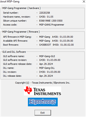
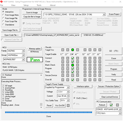
If your hardware connection is correct, I think maybe the txt file you generated on IAR may have some error. Do you do modification on NONMAIN? And can you send your txt file to me? And if we can't resolve it, I will contact with my software team colleague who is responsible for the MSP-GANG.
Best Regards,
Janz Bai
Hello,
1). BSL invoke is not needed when you want to download code using MSP-GANG;
2). I do tests on my side using the two txt files you send to me and I found that I can't download successfully and get the same error with you;
3). It seems that you use XDS110 and download the project directly in IAR and be successfully but when you want to download the txt file into M0 through MSP-GANG, you will get error, so I think that maybe the txt file you generated is wrong or your method to generate txt file is wrong.
4). I generate the txt file of the example code "gpio_toggle_output" in our SDK, you can try to download this file and check whether it will report the error.
e2e.ti.com/.../gpio_5F00_toggle_5F00_output_5F00_LP_5F00_MSPM0G3507_5F00_nortos_5F00_iar.txt
5). If you can, try to use another G307 Lauchpad to do some tests. I think the txt file you send to me (you used) may have some error. Both these two txt files can't be downloaded successfully through MSP-GANG.
6). Please take a video about how you generate the txt file and check whether the SDK you use is the same as the one in IAR
<![if !vml]><![endif]><![if !vml]><![endif]>
Best Regards,
Janz Bai
Dear Janz,
After programming with "gpio_toggle_output" and then use the MSP-GANG to burn other txt file will come with the same error.
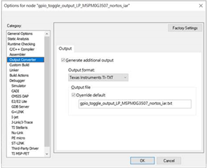
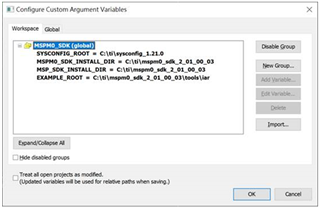
See the picture for the way to generate output file.
Do you think this may cause the problem?
Best Regards,
Eric Chen
Hello Eric,
1), You can let customer use the latest version Uniflash to download his own txt file temporarily. I have tests that using Uniflash can download customer's txt file successfully;
UNIFLASH Software programming tool | TI.com
2). In fact, if you must enter into BSL mode and then download code can be successful, it may caused by that MCU are running to a error state when MSP-GANG want to download code into it. Entering BSL mode can let MCU enter into BSL state and then download code.
3). In fact, I have done some tests on my side today using the txt file generated by SDK example on CCS, just a few times, it reports the same verify error. This error can't be repeated each time so I think that maybe it is caused by hardware reason such as unstable connection, etc. It is so strange and I will contact with my colleague who is responsible for MSP-GANG and ask for his commons. Please wait for a few days, because they are in Thanksgiving Holiday.
Best Regards,
Janz Bai
Hello Eric,
Added more information.
1). Please let customer check his hardware connection and try to download the txt file I sent multi times, check whether it will report the verify error.
2). Please let customer generate the txt file using the same example "gpio_togle_output" as mine through IAR, and download it into MCU through MSP-GANG multi times, check whether it will report the error. After customer generate the txt file. please send it to me too.
Best Regards
Janz Bai
Dear Janz,
Here is the finding from customer side.
Seems that when using MSP-GANG, only burning the same code as the original Flash would work.
1. After burning with "gpio_toggle_output" with XDS110, and then born the same code (gpio_toggle_output) with MSP-GANG works well.
But if we start burning with "05_gpio_toggle_output_LP_MSPM0G3507_nortos_iar" or "20_gpio_toggle_output_LP_MSPM0G3507_nortos_iar". it will occur verify error.
2. After burning with "05_gpio_toggle_output_LP_MSPM0G3507_nortos_iar" with XDS110, and then born the same code (05_gpio_toggle_output_LP_MSPM0G3507_nortos_iar) with MSP-GANG works well.
But if we start burning with "gpio_toggle_output" or "20_gpio_toggle_output_LP_MSPM0G3507_nortos_iar". it will occur verify error.
3. The same flow and result for "20_gpio_toggle_output_LP_MSPM0G3507_nortos_iar".
Best Regards,
Eric Chen
Dear Janz,
Seems to conclusion will be
1.Use the XDS110 first to burn the provided "gpio_toggle_output", use the MSP-GANG to re-flash the same file, repeat 15 times pass
2.Reuse the IAR Compilation Example "gpio_shoot_output" txt file such as an attachment, and use XDS110 first to burn the same file, with MSP-GANG overflash the same file, repeat 15 times pass
@0000
00 04 20 20 A5 02 00 00 33 01 00 00 33 01 00 00
00 00 00 00 00 00 00 00 00 00 00 00 00 00 00 00
00 00 00 00 00 00 00 00 00 00 00 00 33 01 00 00
00 00 00 00 00 00 00 00 33 01 00 00 33 01 00 00
33 01 00 00 33 01 00 00 33 01 00 00 33 01 00 00
33 01 00 00 33 01 00 00 33 01 00 00 33 01 00 00
00 00 00 00 33 01 00 00 33 01 00 00 00 00 00 00
00 00 00 00 33 01 00 00 33 01 00 00 33 01 00 00
33 01 00 00 33 01 00 00 33 01 00 00 33 01 00 00
33 01 00 00 33 01 00 00 00 00 00 00 00 00 00 00
33 01 00 00 33 01 00 00 00 00 00 00 00 00 00 00
33 01 00 00 00 00 00 00 33 01 00 00 33 01 00 00
0F 4A 81 50 70 47 95 22 52 01 81 50 70 47 0D 4A
81 50 70 47 10 B5 00 F0 1F F8 0B 4C 80 21 C9 04
20 00 FF F7 F0 FF 09 49 20 00 FF F7 E9 FF 08 48
00 F0 1A F8 07 49 20 00 FF F7 E9 FF F7 E7 00 00
90 12 00 00 B0 12 00 00 00 20 0A 40 00 00 41 08
00 24 F4 00 00 00 41 0C 80 B5 00 F0 0B F8 00 F0
21 F8 00 F0 3B F8 01 BD 81 1E 09 1F 00 BF FC D2
70 47 FE E7 38 B5 09 4D 28 00 00 F0 5C F8 08 4C
20 00 00 F0 58 F8 28 00 00 F0 50 F8 20 00 00 F0
4D F8 10 20 FF F7 E8 FF 31 BD 00 BF 00 00 0A 40
00 20 0A 40 38 B5 31 20 00 F0 49 F8 38 20 00 F0
46 F8 39 20 00 F0 43 F8 20 20 00 F0 40 F8 05 4D
05 4C 21 00 28 00 00 F0 40 F8 21 00 28 00 00 F0
40 F8 31 BD 00 20 0A 40 00 00 41 0C 80 B5 00 20
00 F0 0E F8 00 20 00 F0 0E F8 00 F0 19 F8 00 F0
11 F8 01 BD 03 68 93 43 0A 40 1A 43 02 60 70 47
15 49 08 60 70 47 80 B5 01 00 03 22 13 48 FF F7
F1 FF 01 BD 12 4A 10 68 12 49 01 40 11 60 70 47
0F 4A 10 68 01 21 88 43 10 60 70 47 0E 4A 80 21
09 01 42 50 70 47 0D 4A 0D 49 42 50 70 47 81 22
0C 49 80 00 08 18 42 60 70 47 95 22 52 01 81 50
70 47 09 4A 81 50 70 47 08 03 0B 40 00 01 0B 40
08 01 0B 40 FF FE FF FF 01 00 00 26 03 00 00 B1
04 08 00 00 00 80 42 40 D0 12 00 00 05 48 01 46
03 B4 68 46 80 F3 09 88 00 BF 00 BF 00 BF 00 BF
00 F0 02 F8 A5 ED F5 FE 00 F0 0D F8 00 28 01 D0
00 BF 00 BF 00 BF 00 BF 00 20 00 BF 00 BF FF F7
31 FF 00 F0 02 F8 01 20 70 47 80 B5 00 F0 02 F8
01 BD 00 00 07 46 38 46 00 F0 02 F8 FB E7 00 00
80 B5 00 BF 00 BF 02 4A 11 00 18 20 AB BE FB E7
26 00 02 00 80 B5 FF F7 C9 FF 01 BD 00 00 00 00
q
Best Regards,
Eric Chen
Hello Eric,
Get it. As I mentioned in the email. Please wait for my colleague Henry to give some commons.
Best Regards,
Janz Bai
Hey Eric,
Thanks for reaching out and apologies for the delay.
From what you're describing it seems like there needs to be an update in the erase process.
It seems like the default erase being done is the sector erase but due to the fact that the latter image is smaller some remnants of the former image remain causing issues. This is why the clear lock device (factory reset) option fixes the issue.
Will follow up with Elprotronic soon and keep you updated.
Henry Nguyen
Hello Eric,
As we talked through email. you can let customer test the latest version MSP-GANG software.
Best Regards,
Janz Bai
Dear Janz,
It can work from my end.
Again, thanks for your support on this!
Best Regards,
Eric Chen
**Attention** This is a public forum