This thread has been locked.

If you have a related question, please click the "Ask a related question" button in the top right corner. The newly created question will be automatically linked to this question.

XT1 MSP430FR5720 problem

Other Parts Discussed in Thread: MSP430FR5720

Hello everybody!

I have a problem with starting XT1 crystal oscillator in 32768 KHz mode on MSP430FR5720. It just does not start. The scope attached to the ACLK monitoring pin shows the VLFO frequency (about 8 KHz). The crystal is designed for 7.5 pF load, I use 9 pF external caps on both XT1 pins. Tried several  cryslats with various load caps in the range 6pf - 12.5 pF and increased external caps up to 20 pF.  Development is done in IAR Workbench, the programmer is MSP-FET430UIF, debugging protocol is Spy-Bi-Wire. The circuit is powered directly from the programmer at 3V.

I tried the code below on FR5730 and FR5728 with no luck. The last two lines in this snipplet are modified from the example code msp430fr57xx_LPM3_01.s43 and others from the same examples set where XF1 is used. The original lines in these examples

            cmp.w   #0x01,&OFIFG        ; Test oscillator fault flag
            jz            OSCFlag

do not make sense for me since OFFIFG is not a valid SFR name. I tried these lines anyway, but it does not work too. The debugger shows both flags XT1OFFG and OFIFG are set no matter how long I cycle in the oscillator starting loop. Here is my code.

reset:  mov .w    #SFE(CSTACK), SP                          ; set up stack
            mov.w     #WDTPW+WDTHOLD, &WDTCTL ; stop watchdog timer

            mov.w     #0x0F, &PJDIR
            bis.w      #BIT5+BIT4, &PJSEL0                       ; enable Xtal oscillator pins

            bis.w      #BIT2, &PJSEL0                                  ; enable ACLK monitoring pin

            mov.b     #0xA5, &CSCTL0_H                           ; unlock the clock interface
            mov.b     #XT1DRIVE_3, &CSCTL4_L             ; crystal drive level  (tried _0 - _3)                  

wco1:   bic.w    #XT1OFFG, &CSCTL5                        ; clear XT1 fault flag
              bic.w    #OFIFG, &SFRIFG1       
              bit.w    #OFIFG, &SFRIFG1                             ; test oscillator fault flag
              jnz        wco1                                                      ; wait for crystal osc. to start

I would appreciate any advise for a direction to follow. The problem drives me crazy, as everything else works fine with VLFO if I disable the last jnz instruction.

  • Serguei Bezroukov said:
    The crystal is designed for 7.5 pF load, I use 9 pF external caps on both XT1 pins. Tried several  cryslats with various load caps in the range 6pf - 12.5 pF and increased external caps up to 20 pF.


    For 7.5pF load, the external caps need to be (2*15pF -2*2pF pin capacitance) = 2*13pF.

    The pad logic for PJ.4/PJ.5 shows that XIN/XOUT is always selected. However, setting PJSEL.4/5 disables the input and output driver and the pullup.

    However, the code shoul dwork. If it doesn't, my first bet would be a hardware problem. Did you try different crystals?
    We too had problems with crystals (8MHZ) on several devices - with a firmware that worked flawlessly before and was unchanged for years. Replacing the crystals usually helped. We dstill don't know what the exact problem was, but with our $700 probe we were able to observe that the 'good' ones ocillated with >+-0.6V while the bad ones just hat <+-0.1V oscillation.

    However, don't forget the parasitic capacitance of teh PCB traces, ans especially of a GND layer on the backside. (there shouldn't be a GND layer right beneath the traces).

  • Thanks for a prompt reply.

    > For 7.5pF load, the external caps need to be (2*15pF -2*2pF pin capacitance) = 2*13pF.

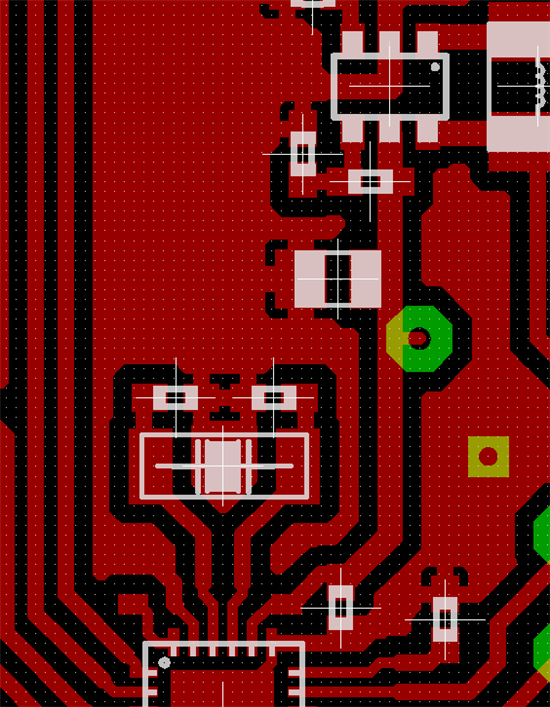
    It is difficult for me to evaluate the parasitic capacitance. I assumed it is about 5pF/pin including the traces. Below is a part of my board design (the MSP430 is in the bottom part of it, QFN package). The distance between the dots is 0.25mm. But as far as I understand, a slight mismatch in the crystal load caps value should just lead to some offset in oscillation frequency and it should oscillate anyway. I need to use low-profile components, so the 0805 cap is the highest part on board. The crystal is Abracon in ABS09 package. I also tried one in ABS07 package and a one in a match package from Citizen:

    http://www.abracon.com/Resonators/ABS07.pdf   and   http://cfm.citizen.co.jp/english/product/pdf/CMJ206T.pdf

    What crystal would you recommend?

    The board is 2-sided, the other side is solid copper background plain in accordance with SLAA322b:

    "With 2-layer boards, do not route any digital-signal lines on the opposite side of the PCB under the crystal area. In any case, it is good design practice to fill the opposite side of the PCB with clean ground and also connect this ground to AVSS of the MSP430."

    If I touch XT1 pin right after powering the circuit, it oscillates on the right frequency (+ some noise). Bus as soon as I remove the finger it switches back to VLFO (8 KHz) and further touches do not turn it back to 32kHz. The program at this time is looping in the "wait and pray" loop for XF1 to start.  The DC voltage on XT1 pin is about 0.2V and the one on XT1 is 0.6V, no oscillation is noticed. Maybe it would make sense to try to put a resistor in parallel with the crystal to tune the linear mode of the oscillator inverter? I tried 3Mom, but it did not work.

    I understand the logic behind the PJSEL0 register. I also understand the reason for the XT1OFFG flag in CSCTL5. Section 3.2.7 in the datasheet tells that "fault is detected, the system clock is automatically switched to the VLO". What I do not understand is how to force the system to switch back to XF1 after it finally starts? In the clock waiting loop from my first post I clear the fault flags but they are rise up again right away. A 1-sec delay between clearing the flags and checking then does not help.

    Is there any way to "kick" the XF1 forcing it to try to start again? Maybe do a software reset or something?

  • Serguei Bezroukov said:
    But as far as I understand, a slight mismatch in the crystal load caps value should just lead to some offset in oscillation frequency and it should oscillate anyway.

    Frequency and amplitude of the oscillation are affected. Whiel amplitude isn't a problem for accuracy, it is a problem if it gets too low :)

    Serguei Bezroukov said:
    Is there any way to "kick" the XF1 forcing it to try to start again

    No need to. The Pierce Oscillator is based on an inverter. As soon as the voltage on the inverter input crossses the threshold, it switches its output, causing the voltage on the input to change into opposite direction (delayed and controlled by the crystal and the load capacitance). So there is no 'starting kick'. As soon as the inverter is active it will always oscillate as soon as its output influences its input. Shortcutting the two pins will result in HF oscillation based on the inverters internal propagation delay and parasitic capacitance of the pins and the input transistor.

    Serguei Bezroukov said:
    What I do not understand is how to force the system to switch back to XF1 after it finally starts

    Successfully clearing OFIFG causes the switch back form fallback to workign oscillator. This is why a second touch doesn't help. The first touch allows your loop to exit and XT1 is working. If you now remove the finger, XT1OFFG and OFIFG are set and VLO is activated as fallback. Now you never clear them again in your code, so it will never switch back to XT1 even if it is working.

    You'll need to write an NMI function that reacts on OFIFG (enabled by OFIE) and either periodically or instantly (busy loop) tries to reset those bits.

    Serguei Bezroukov said:
    In the clock waiting loop from my first post I clear the fault flags but they are rise up again right away

    the fault flags are write-protected (cannot be cleared) as long as the fault condition still exists. You can only clear them if no fault has been detected for the last n oscillator cycles (on F5x family, 8192 clock ticks for the LFXT1, I don't know off-hand  for FR5x.)
    This is different from 1x family (and 2x?) clock system, where you could reset them but they were set again after the fault timeout expired again, so you had to use a delay.

  • Thank you very much, it was a very useful discussion that helped me to understand the XF1 logic better. I also got a feeling that the XT1OFFG and OFIFG bits are write protected. If I stop the XF1 in the waiting loop by setting  XT1OFF bit in CSCTL4 then I can successfully reset XT1OFFG and OFIFG bits as the debugger shows. But as I reset XT1OFF bit at the end of waiting loop, the XT1OFFG and OFIFG are set right away automatically, signalling that XT1 is not oscillating.

    I have managed to start XT1 with that crystal and above code on a one-sided test board that has no copper below the XF1 elements. But on the board in question (that has a solid copper on one side) XT1 does not oscillate at all even if I short cut the crystal with a wire jumper. It is strange because the MSP430FR57xx Experimenter Board has solid copper below the crystal. Anyway, you are right that I got a hardware problem. I ordered several types of crystals and it will take some time to find an appropriate layout.  

  • Serguei Bezroukov said:
    XT1 does not oscillate at all even if I short cut the crystal with a wire jumper.

    Hmmm, it should (well, with really high frequency and rather small amplitude, around the inverters input trigger level)

    Do you have perhaps a shortcut between teh XT1 pisn and adjacent pins (maybe beneath the FR)? Happened a few times on out boards too.

    For the layout, well, we have a copper plane on the backside too, but not right beneath the traces to the crystal. Also, even if one wouldn't think so, currents have preferred paths even on a copper plane. And the HF form the crystal and its traces is attracting currents on the copper plane - which in turn influence the oscillation. So the area between the traces from chip to crystal is an isolated pad that is connected to the copper plane only at the point where the capacitors meet GND on the upper side. Where the signal traces are on the upside is the gap around this island on the downside. Well, that's for our 8MHz crystals. But the 32kHz isn't that different (except that on most MSPs no caps are required for the 32kHz crystals).

  • I checked the resistance between the XF1 pins and the others around. It shows several MOMs, so there is definitely no shortcut. However, it is possible that there is some amount of flux below the QFN24 package whose resistance could mess up the linear mode of the oscillator inverter. Some invertor-based crystal oscillators have a resistor between its output and input, you know.. I am not sure if it is the case for FR57xx, but could the flux residuals influence the start of XF1? I solder my chips manually and it is hard to me to guarantee the absence of flux below the chip. The used flux is Kester #2331, I applied water to remove it afterwards and dried the board for about a minute under a fan. I am pretty mch certain there is no water drops below the chip left, but cannot guarantee the flux absence. I investigated the near chip area under a 50x microscope - everything looks fine to me, although I cannot see what is below the chip.

    Anyway, as I wrote, I ordered several crystals and am going to experiment next week with various board lauouts with and without ground plain under the crystal pins area. It is hard for me to reproduce the layout you mentioned, but I will try. One more thing: do you recommend to connect AVSS pin to the QFN chip exposed pad under the chip? I did it on the one-sided board where XF1 works now and did not do it on the problematic 2-sided board. i am not sure if it makes any difference, in general. I am not concerned with the accuracy of ADC - all I need it to start XF1. BTW, can grounding of the exposed pad of QFN packages influence of XF1 stability? I did not solder exposed pads on my both boards.   

  • I would suggest connecting the exposed pad under the device to ground.

  • OK, I figured it out. It was a soldering problem. After lifting the chip up I discovered traces of some liquid under it. I cleaned the PCB and the chip and soldered the chip back, but this time with hot air gun instead of a soldering iron. It looks to me that the flux residuals are vaporized now because of the heat. At least I did not even need to clean them out of the PCB. Anyway, the XT1 oscillates with the same crystal (Abracon ABS09-32.768KHZ-7-T), 12pF capacitors, and the layout as on the image above. The crystal load is not 7.5 pF as I mentioned by mistake earlier, but just 7pF. Here is my XT1 waiting loop for reference.

     mov.b   #0xA500, &CSCTL0_H   ; unlock the clock interface
       mov.b   #XT1DRIVE_1, &CSCTL4_L ; set crystal drive strength
    wco: bic.b   #XT1OFFG, &CSCTL5_L     ; clear XT1 fault flags
            bic.b   #OFIFG, &SFRIFG1_L
            bit.b   #OFIFG, &SFRIFG1_L     ; test oscillator fault flag
         jnz     wco                     ; wait for crystal osc. to start

    Many thanks to everybody for a helpful and stimulating discussion. I will solder the exposed pad next time.

**Attention** This is a public forum