This thread has been locked.

If you have a related question, please click the "Ask a related question" button in the top right corner. The newly created question will be automatically linked to this question.

Internal Pull-up Resistors on MSP430x2xx and LaunchPad

Other Parts Discussed in Thread: MSP430G2553

Hi,

I've just received the Launchpad board, with MSP430x2xx, and I'm a bit confused with the User Guides and Datasheets...

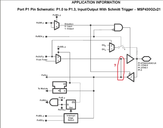
It's said that the MSP430x2xx series include internal pull-up/pull-down resistors, and these are configured with PxREN registers.

Although, when I look at the Launchpad User's Guide, on the board's schematic, there are 47kOhm pull-up resistors tied to Vcc on Port P1.3 and RST.

Are the pull-up resistors really internal, or do I need to connect a 47kOhm resistor in every port used as input? If I don't connect these resistors, and only insert a button, will I have my microcontroller damaged?

Thanks,

Fernando

  • In this regard, the user's guide and data-sheets are correct.

    To include external pull-up is optional but usually unnecessary. The 47K pull-up resistor at P1.3 on the Launchpad is unnecessary.

    (RST is not a port pin and has no internal pull-up. The external pull-up on the Launchpad for RST pin is necessary.)


  • I haven't checked the schematics, but on many MSPs, the pullups (if available at all) are disabled if the port pin is set to output. While this is obvious for normal I/O, this is important if you use the I2C controller where the output drives only to GND but not to VCC (open collector). If using I2C, you cannot rely on the internal pullups (which are too weak anyway) and need external pullups.

    old_cow_yellow said:
    The 47K pull-up resistor at P1.3 on the Launchpad is unnecessary.

    It depends. the itnernal up to 50k may be too weak for some purposes, maybe it is a relic from a planned  add-on on the LaunchPad. maybe debouncing for a pushbutton, maybe, well, whatever.

    old_cow_yellow said:
    RST is not a port pin and has no internal pull-up. The external pull-up on the Launchpad for RST pin is necessary.

    The 5x/6x family has pullup/pulldown on the RST/NMI pin, but on some (54xx non-A) it isn't enabled as pullup by default.

  • This is the doc from the x2xxFamilyGuide-slau144e.pdf family guide.  

    8.2.4 Pullup/Pulldown Resistor Enable Registers PxREN

    Each bit in each PxREN register enables or disables the pullup/pulldown


    resistor of the corresponding I/O pin. The corresponding bit in the PxOUT

    register selects if the pin is pulled up or pulled down.

    Bit = 0: Pullup/pulldown resistor disabled

    Bit = 1: Pullup/pulldown resistor enabled


    So I guess you write to the PxOUT register even though the port is configured as input to control the pullup or pulldown effect for input.  For output, it looks like it would act as a very high impedance digital source I think.

    But I don't understand the connection I highlighted in red.  It seems to conflict with the input buffer output????  How does that work?

    -SB


  • I do not think you can take those “schematics” literally. The connection you circled in red seems to indicate the existence of a so-called bus-holder (or bus-keeper) there.

  • old_cow_yellow said:

    I do not think you can take those “schematics” literally. The connection you circled in red seems to indicate the existence of a so-called bus-holder (or bus-keeper) there.

    Would that imply that the "PxSEL.y" device has a high impedance output that can be easily overridden by the input Schmitt Trigger buffer?  Somehow that seems at odds with the extreme low-power design of the MSP430 devices because overriding gates would seem to waste power.

    -SB

  • s b said:
    Each bit in each PxREN register enables or disables the pullup/pulldown

    This is true for this particular MSP, but on other MSPs (e.g. the 54xx), the PxREN signal is connected with the PxDIR signal, disabling the pullups when the pin is output.

    Here, it looks like PxREN will disable the output driver completely.

    For the red connection, well, you will only have input or output active at a time, so it might make sense. the pin is output, the input driver is off, and the PxIN bit (and all othe rinputs) follow the output, without causing any current consumption by the input. It gives you lowest curent consumption if you set all unused pins to low outputs.
    If the pin is input, however, there shouldn't be an output singal on this line (the PxSEL switch should be high-impedance then). So eithe rOCY is right and this is a bus keeper circuit rather than a direct connection, or there is a PxDIR controlled buffer missing on this line.


  • Jens-Michael Gross said:

    Here, it looks like PxREN will disable the output driver completely.

    Yes, the output will be only a trickle through the pullup/down resistor it looks like.

    Jens-Michael Gross said:

    For the red connection, well, you will only have input or output active at a time, so it might make sense. the pin is output, the input driver is off, and the PxIN bit (and all othe rinputs) follow the output, without causing any current consumption by the input. It gives you lowest curent consumption if you set all unused pins to low outputs.
    If the pin is input, however, there shouldn't be an output singal on this line (the PxSEL switch should be high-impedance then). So eithe rOCY is right and this is a bus keeper circuit rather than a direct connection, or there is a PxDIR controlled buffer missing on this line.

    Ok, thanks.

    BTW: I'm not clear on how the "bus keeper" connection looks schematically.  I thought it was basically a wire with side latch that holds the last value weakly if both ends go high impedance.  It would still seem to connect two outputs together (input buffer and PxSEL.y switch) and during input mode, both outputs would not be high impedance (I don't see why PxSEL.y would be high impedance in input mode).

    -SB

  • s b said:
    I don't see why PxSEL.y would be high impedance in input mode

    No it isn't. I meant it better should if there is such a direct connection.

  • Jens-Michael Gross said:

    I don't see why PxSEL.y would be high impedance in input mode

    No it isn't. I meant it better should if there is such a direct connection.

    [/quote]

    Ok, that makes sense.

  • This may be a redundant question, but I just want to ensure. I am using a MSP430G2553 with the P1.6 and P1,7 pins for I2C. So is it necessary to connect an external pull up resistor? If yes, is 4.7k enough?

    Thanks.

  • Sivashyam Sundar A said:
    I am using a MSP430G2553 with the P1.6 and P1,7 pins for I2C. So is it necessary to connect an external pull up resistor? If yes, is 4.7k enough?

    Depending on teh bus topology (number of slaves, signal length) a pullup of 1k to 10k is required. (10k for only one slave and not too long traces). The internal pullups of 37-50k, even though not disabled when the pin is in output direction, are too weak.
    However, you may combine them to improve signal quality: put the external pullup near the slave and enable the MSPs internal pullup. This may (!) result in better performance. Or the opposite :) It depends on the schematic.

  • Dear freinds

    Just would like to check if I am doing the right thing. I am using the UART for communicating between the MSP430G2553 and BNO055 accelerometer. I am doing these settings for the pins, would you please advice if I am doing the right settings with the aim to set any unused pin to input/ no pull up, no pull down resister? I care about pins settings as I would like to run the system from a battery and thus energy consumption is a concern for me.


    Thank you

    // P1.1 = RXD, P1.2=TXD defined in the .h file
    
    P1IE &= ~(RXD + TXD);	// Disable interrupt
    P1REN &= ~(TXD); // Disable pullup/pulldown resistor
    P1DIR |= TXD; // Set as output
    P1OUT &= ~TXD;
    P1SEL |= RXD + TXD ; // P1.1 = RXD, P1.2=TXD
    P1SEL2 |= RXD + TXD ; // P1.1 = RXD, P1.2=TXD

  • There is no need to configure TX as output since the direction is set by the USCI module and DIR becomes don't care once SEL(2) is set.
  • Yep, setting PxSEL for USCI (but only for USCI, not for other modules) will override PxDIR. And PxREN as well as PxIE are clear by default. So PxOUT is a don't care too (would affect the pull-up if PxREN were set (on some MSPs, setting PxDIR to output will disable the pull-up, but not on the G2553 - yet the pull-up is to week for being used for I2C, where this would be useful)

    Regarding energy consumption, the consumption of the TxD pin is mainly determined by teh attached (external) load.
    It would be a good idea to enable the pull-up for the RX pin. Idle signal line is high anyway, so it only adds some 50 ~µA when the line is active. But it prevents additional consumption when the input is unconnected.
    All other (unconnected) pins should be set to low outputs, as this disables the input logic and prevents input gate fluctuations which may cause unwanted current draw in the input circuitry.
  • OK thanks, and what about the + i am using, should I replace them with logical (||)?

    Actually I got this advice from a friend, but when replacing each + with ||, seems the UART is not working and can not see any TX or RX in the UART buffers!

  • It is not the double "||" OR, it has to be a single one "|" - I would also go for the "|" instead of the "+".
  • "should I replace them with logical (||)"
    As you correctly named it, '||' is the logical OR. It takes two expressions and results in a true or false as result. Which surely isn't what you need.
    As Dennis correctly stated, the binary or is '|'. It logically combines binary bits rather than logical expressions.

    And yes, if you are setting/clearing bits, a binary operator is preferred over a numerical one. Since you can set/clear a bit only once (by using ht ebinary operators). Setting it another time doesn't make a change. But you can numerically add or subtract a bit value multiple times and each time the result is different. The compiler doesn't know what you want to do. It just does what you type. And for the compiler, bit values are numerical values and v.v. Only the operator you use makes the difference.
  • Dears


    Are there specific pin(s) associated with I2C or USCI Bx in MSP430G2553?

    Can I use pin 1.1 & 1.2 for I2C communications?

    I used them before for UART and they worked fine, now I am switching to I2C and thus little bit confused as I thought that each communication interface has its own associated pins!

    Thank you

  • To answer questions like this, TI has designed something called 'data sheet'. :)

    The G2553 data sheet tells that the UCB0SDA signal is available on P1.7 while UCB0SCL is connected to P1.6.
    P1.1/1.2 are the signal pins for UCA. According to the user's guide (and it's right, here, I tested!), the USCI A module supports either UART or SPI (and the two indeed share the same pins) while USCI B module supports I2C and SPI (also on the same pins).
    Since SPI requires at least 3 signals, each USCI(A/B) has a third pin for clock, which is shared with the optional 4th SPI signal (STE) of the other USCI(A/B).
    Bigger MSPs have multiple USCI(A/B) pairs with their own set of 6 pins and in some cases an additional 'half' USCI(A) (probably the associated USCIB just has no pins assigned).
    Some MSPs from 5x family do have a port mapping module that allows routing of the signals to different pins.


    But...

    Of course you can use P1.1/P1.2 for I2C communication. You just have to do it completely in software (sometimes the better choice compared to a hardware re-design). Just like the BSL on the G2553 does the UART communication in software on these pins. Implementing a simple I2C master isn't difficult. But it's easier to use P1.6/P1.7 with hardware support.

**Attention** This is a public forum