This thread has been locked.

If you have a related question, please click the "Ask a related question" button in the top right corner. The newly created question will be automatically linked to this question.

MSP430G2131: SPI communication

Part Number: MSP430G2131
Other Parts Discussed in Thread: DRV8838

Hi, 

We are trying to establish SPI between MSP430G2131(slave) and CH341A(master) to control the potentiometer. The goal is to read the potentiometer data from the DRV8838 EVM board and transfer it from the slave to the master.

To verify that the MSP430G2131 chip works correctly as a slave, I am currently establishing a SPI communication between 2 MSP430G2131 chips.

I have a few questions as below:

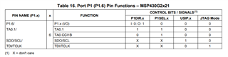
  • Page 403 of the msp430x_2xx user guide (pdf) mentions


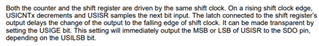
  1. Is there any difference between the shift clock and the SMCLK?
  2. Why are we given an option to configure USICKPH and USICKPL if it is fixed that USICNTx decrements and USISR samples the next bit input on the rising clock edge?


  • I am a little confused about the difference between PxIN, PxOUT, PxDIR and PxSEL registers.

For instance, in the example codes:

SPI Slave config

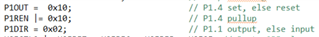
  1. How can we configure ‘P1.1 as output rest input’ in P1DIR and then set P1.4 in P1OUT? Does that mean both of the pins are acting as inputs?


SPI Master config

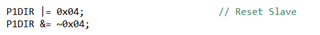
  1. How is P1DIR used to reset the slave?


DRV8838_CstomerEVM_Default _Code

  1. What is the function of the above statements?
  2. What is the difference between P1SEL and P1DIR and P1OUT?


  • I am trying to send hardcoded values from the master to the slave and vice-versa. I can see the waveform on P1.6 pin (of MSP430G2131) after I hardcode a value of the USISRL register but not if I hardcode it into the P1OUT register. Doesn’t USISRL register transfer the data to the P1OUT register before transferring?


  • Hi,

    1. Shift clock and SMCLK are totally different tings. Shift clock is only used in the USI peripheral. But the SMCLK is sub system clock, it provides clock resource for most on-chip peripherals. See the figure 14.1 USI block diagram.

    2. Control bit USICKPL selects the inactive level of the SPI clock while USICKPH selects the clock edge on which SDO is updated and SDI is sampled. Based on the UG 14.2.3  SPI mode

    3. You can find the useful information about these registers PxIN, PxOUT, PxDIR and PxSEL in UG chapter 8.2 Digital I/O Operation. 

    Which example code you are using here? I found there are two examples codes related to the SPI function. None of these two looks the same as you shown.

    msp430g2x21_usi_05.c
    /* --COPYRIGHT--,BSD_EX
     * Copyright (c) 2012, Texas Instruments Incorporated
     * All rights reserved.
     *
     * Redistribution and use in source and binary forms, with or without
     * modification, are permitted provided that the following conditions
     * are met:
     *
     * *  Redistributions of source code must retain the above copyright
     *    notice, this list of conditions and the following disclaimer.
     *
     * *  Redistributions in binary form must reproduce the above copyright
     *    notice, this list of conditions and the following disclaimer in the
     *    documentation and/or other materials provided with the distribution.
     *
     * *  Neither the name of Texas Instruments Incorporated nor the names of
     *    its contributors may be used to endorse or promote products derived
     *    from this software without specific prior written permission.
     *
     * THIS SOFTWARE IS PROVIDED BY THE COPYRIGHT HOLDERS AND CONTRIBUTORS "AS IS"
     * AND ANY EXPRESS OR IMPLIED WARRANTIES, INCLUDING, BUT NOT LIMITED TO,
     * THE IMPLIED WARRANTIES OF MERCHANTABILITY AND FITNESS FOR A PARTICULAR
     * PURPOSE ARE DISCLAIMED. IN NO EVENT SHALL THE COPYRIGHT OWNER OR
     * CONTRIBUTORS BE LIABLE FOR ANY DIRECT, INDIRECT, INCIDENTAL, SPECIAL,
     * EXEMPLARY, OR CONSEQUENTIAL DAMAGES (INCLUDING, BUT NOT LIMITED TO,
     * PROCUREMENT OF SUBSTITUTE GOODS OR SERVICES; LOSS OF USE, DATA, OR PROFITS;
     * OR BUSINESS INTERRUPTION) HOWEVER CAUSED AND ON ANY THEORY OF LIABILITY,
     * WHETHER IN CONTRACT, STRICT LIABILITY, OR TORT (INCLUDING NEGLIGENCE OR
     * OTHERWISE) ARISING IN ANY WAY OUT OF THE USE OF THIS SOFTWARE,
     * EVEN IF ADVISED OF THE POSSIBILITY OF SUCH DAMAGE.
     *
     *******************************************************************************
     * 
     *                       MSP430 CODE EXAMPLE DISCLAIMER
     *
     * MSP430 code examples are self-contained low-level programs that typically
     * demonstrate a single peripheral function or device feature in a highly
     * concise manner. For this the code may rely on the device's power-on default
     * register values and settings such as the clock configuration and care must
     * be taken when combining code from several examples to avoid potential side
     * effects. Also see www.ti.com/grace for a GUI- and www.ti.com/msp430ware
     * for an API functional library-approach to peripheral configuration.
     *
     * --/COPYRIGHT--*/
    //******************************************************************************
    //  MSP430G2x21/G2x31 Demo - USI SPI Interface to TLC549 8-bit ADC
    //
    //   Description: This program demonstrates the USI in SPI mode interface to a
    //   TLC549 8-bit ADC. If AIN > 0.5(REF+ - REF-), P1.0 set, else reset.
    //   ACLK = n/a, MCLK = SMCLK = default DCO, UCICLK = SMCLK/4
    //   //** VCC must be at least 3v for TLC549 **//
    //
    //                       MSP430G2x21/G2x31
    //                       -----------------
    //                   /|\|              XIN|-
    //        TLC549      | |                 |
    //    -------------   --|RST          XOUT|-
    //   |           CS|<---|P1.1             |
    //   |      DATAOUT|--->|P1.7/SOMI    P1.0|-->LED
    // ~>|AIN   I/O CLK|<---|P1.5/SCLK        |
    //
    //  D. Dang
    //  Texas Instruments Inc.
    //  October 2010
    //  Built with CCS Version 4.2.0 and IAR Embedded Workbench Version: 5.10
    //******************************************************************************
    
    #include <msp430.h>
    
    
    int main(void)
    {
      WDTCTL = WDTPW + WDTHOLD;                 // Stop watchdog timer
      P1OUT = 0;
      P1DIR |= 0x03;
      USICTL0 |= USIPE7 + USIPE5 + USIMST + USIOE; // Port, SPI master
      USICTL1 |= USIIE;                         // Counter interrupt, flag remains set
      USICKCTL = USIDIV_2 + USISSEL_2;          // /4 SMCLK
      USICTL0 &= ~USISWRST;                     // USI released for operation
      USICNT = 8;                               // init-load counter
      __bis_SR_register(LPM0_bits + GIE);       // Enter LPM0 w/ interrupt
    }
    
    // USI interrupt service routine
    #if defined(__TI_COMPILER_VERSION__) || defined(__IAR_SYSTEMS_ICC__)
    #pragma vector=USI_VECTOR
    __interrupt void universal_serial_interface(void)
    #elif defined(__GNUC__)
    void __attribute__ ((interrupt(USI_VECTOR))) universal_serial_interface (void)
    #else
    #error Compiler not supported!
    #endif
    {
      P1OUT |= 0x02;                            // Disable TLC549
      if (USISRL > 0x7F)
        P1OUT |= 0x01;
      else
        P1OUT &= ~0x01;
      P1OUT &= ~0x02;                            // Enable TLC549
      USICNT = 8;                                // re-load counter
    }
    

    msp430g2x21_usi_04.c
    /* --COPYRIGHT--,BSD_EX
     * Copyright (c) 2012, Texas Instruments Incorporated
     * All rights reserved.
     *
     * Redistribution and use in source and binary forms, with or without
     * modification, are permitted provided that the following conditions
     * are met:
     *
     * *  Redistributions of source code must retain the above copyright
     *    notice, this list of conditions and the following disclaimer.
     *
     * *  Redistributions in binary form must reproduce the above copyright
     *    notice, this list of conditions and the following disclaimer in the
     *    documentation and/or other materials provided with the distribution.
     *
     * *  Neither the name of Texas Instruments Incorporated nor the names of
     *    its contributors may be used to endorse or promote products derived
     *    from this software without specific prior written permission.
     *
     * THIS SOFTWARE IS PROVIDED BY THE COPYRIGHT HOLDERS AND CONTRIBUTORS "AS IS"
     * AND ANY EXPRESS OR IMPLIED WARRANTIES, INCLUDING, BUT NOT LIMITED TO,
     * THE IMPLIED WARRANTIES OF MERCHANTABILITY AND FITNESS FOR A PARTICULAR
     * PURPOSE ARE DISCLAIMED. IN NO EVENT SHALL THE COPYRIGHT OWNER OR
     * CONTRIBUTORS BE LIABLE FOR ANY DIRECT, INDIRECT, INCIDENTAL, SPECIAL,
     * EXEMPLARY, OR CONSEQUENTIAL DAMAGES (INCLUDING, BUT NOT LIMITED TO,
     * PROCUREMENT OF SUBSTITUTE GOODS OR SERVICES; LOSS OF USE, DATA, OR PROFITS;
     * OR BUSINESS INTERRUPTION) HOWEVER CAUSED AND ON ANY THEORY OF LIABILITY,
     * WHETHER IN CONTRACT, STRICT LIABILITY, OR TORT (INCLUDING NEGLIGENCE OR
     * OTHERWISE) ARISING IN ANY WAY OUT OF THE USE OF THIS SOFTWARE,
     * EVEN IF ADVISED OF THE POSSIBILITY OF SUCH DAMAGE.
     *
     *******************************************************************************
     * 
     *                       MSP430 CODE EXAMPLE DISCLAIMER
     *
     * MSP430 code examples are self-contained low-level programs that typically
     * demonstrate a single peripheral function or device feature in a highly
     * concise manner. For this the code may rely on the device's power-on default
     * register values and settings such as the clock configuration and care must
     * be taken when combining code from several examples to avoid potential side
     * effects. Also see www.ti.com/grace for a GUI- and www.ti.com/msp430ware
     * for an API functional library-approach to peripheral configuration.
     *
     * --/COPYRIGHT--*/
    //******************************************************************************
    //  MSP430G2x21/G2x31 Demo - USI SPI Interface with HC165/164 Shift Registers
    //
    //  Description: Demonstrate USI in two-way SPI mode. Data are read from
    //  an HC165, and same data written back to the HC164.
    //  ACLK = n/a  MCLK = SMCLK = default DCO, USICLK = SMCLK/2
    //  //*USART0 control bits are in different SFR's from other MSP430's//
    //
    //                       MSP430G2x21/G2x31
    //                       -----------------
    //                   /|\|              XIN|-
    //                    | |                 |     ^      HC164
    //          HC165     --|RST          XOUT|-    |  -------------
    //        ----------    |                 |     |-|/CLR,B       |  8
    //    8  |      /LD|<---|P1.1   SIMO0/P1.6|------>|A          Qx|--\->
    //   -\->|A-H   CLK|<---|P1.5/SCLK0 - P1.5|------>|CLK          |
    //     |-|INH    QH|--->|P1.7/SOMI0       |       |             |
    //     |-|SER      |    |                 |       |             |
    //     - |         |    |                 |       |             |
    //
    //  D. Dang
    //  Texas Instruments Inc.
    //  October 2010
    //  Built with CCS Version 4.2.0 and IAR Embedded Workbench Version: 5.10
    //******************************************************************************
    
    #include <msp430.h>
    
    int main(void)
    {
      WDTCTL = WDTPW + WDTHOLD;                 // Stop WDT
    
      P1OUT = 0;
      P1OUT |= 0x02;
      P1DIR |= 0x02;
      USICTL0 |= USIPE7 + USIPE6 + USIPE5 + USIMST + USIOE; // Port, SPI Master
      USICTL1 |= USICKPH + USIIE;               // Counter interrupt, flag remains set
      USICKCTL = USIDIV_1 + USISSEL_2;          // /2 SMCLK
      USICTL0 &= ~USISWRST;                     // USI released for operation
      USICNT = 8;                               // init-load counter
    
      while (1)                                 // Loop
      {
        unsigned i;
        for (i = 0xFFFF; i > 0; i--);           // Delay
        while (!(USIIFG & USICTL1));            // Counter clear?
        P1OUT &= ~0x02;                         // Latch data into 'HC165
        P1OUT |= 0x02;
    //  ********************                    // Read data are ready to be written
        USICNT = 8;                             // re-load counter
      }
    }
    

    Best regards,

    Cash Hao

  • Hi, 

    1. We are using msp430g2x21_5F00_usi_5F00_02.c and msp430g2x21_5F00_usi_5F00_03.c to establish SPI communication between 2 MSP430G2131 chips.

    2. We have read about the registers PxIN, PxOUT, PxDIR and PxSEL in UG chapter 8.2 Digital I/O Operation. However, their exact function is still not clear to us. Please advise if you can elaborate. 

    Thank you, 

    Piyusha 

  • Hi Piyusha,

    1. Could you share the code you used here? I couldn't find it on our web.

    2. Do you mean you need this following table for how to configure these registers? you can find these registers in the device datasheet.

    Best regards,

    Cash Hao

  • Hi Cash, 

    Below is the code : 

    7776.msp430g2x21_usi_02.c
    /* --COPYRIGHT--,BSD_EX
     * Copyright (c) 2012, Texas Instruments Incorporated
     * All rights reserved.
     *
     * Redistribution and use in source and binary forms, with or without
     * modification, are permitted provided that the following conditions
     * are met:
     *
     * *  Redistributions of source code must retain the above copyright
     *    notice, this list of conditions and the following disclaimer.
     *
     * *  Redistributions in binary form must reproduce the above copyright
     *    notice, this list of conditions and the following disclaimer in the
     *    documentation and/or other materials provided with the distribution.
     *
     * *  Neither the name of Texas Instruments Incorporated nor the names of
     *    its contributors may be used to endorse or promote products derived
     *    from this software without specific prior written permission.
     *
     * THIS SOFTWARE IS PROVIDED BY THE COPYRIGHT HOLDERS AND CONTRIBUTORS "AS IS"
     * AND ANY EXPRESS OR IMPLIED WARRANTIES, INCLUDING, BUT NOT LIMITED TO,
     * THE IMPLIED WARRANTIES OF MERCHANTABILITY AND FITNESS FOR A PARTICULAR
     * PURPOSE ARE DISCLAIMED. IN NO EVENT SHALL THE COPYRIGHT OWNER OR
     * CONTRIBUTORS BE LIABLE FOR ANY DIRECT, INDIRECT, INCIDENTAL, SPECIAL,
     * EXEMPLARY, OR CONSEQUENTIAL DAMAGES (INCLUDING, BUT NOT LIMITED TO,
     * PROCUREMENT OF SUBSTITUTE GOODS OR SERVICES; LOSS OF USE, DATA, OR PROFITS;
     * OR BUSINESS INTERRUPTION) HOWEVER CAUSED AND ON ANY THEORY OF LIABILITY,
     * WHETHER IN CONTRACT, STRICT LIABILITY, OR TORT (INCLUDING NEGLIGENCE OR
     * OTHERWISE) ARISING IN ANY WAY OUT OF THE USE OF THIS SOFTWARE,
     * EVEN IF ADVISED OF THE POSSIBILITY OF SUCH DAMAGE.
     *
     *******************************************************************************
     * 
     *                       MSP430 CODE EXAMPLE DISCLAIMER
     *
     * MSP430 code examples are self-contained low-level programs that typically
     * demonstrate a single peripheral function or device feature in a highly
     * concise manner. For this the code may rely on the device's power-on default
     * register values and settings such as the clock configuration and care must
     * be taken when combining code from several examples to avoid potential side
     * effects. Also see www.ti.com/grace for a GUI- and www.ti.com/msp430ware
     * for an API functional library-approach to peripheral configuration.
     *
     * --/COPYRIGHT--*/
    //******************************************************************************
    //  MSP430G2x21/G2x31 Demo - SPI full-Duplex 3-wire Master
    //
    //  Description: SPI Master communicates full-duplex with SPI Slave using
    //  3-wire mode. The level on P1.4 is TX'ed and RX'ed to P1.0.
    //  Master will pulse slave reset for synch start.
    //  ACLK = n/a, MCLK = SMCLK = Default DCO
    //
    //  **** used with "msp430g2x21_usi_03.c"   ****
    //
    //                Slave                      Master
    //             MSP430G2x21/G2x31          MSP430G2x21/G2x31
    //             -----------------          -----------------
    //            |              XIN|-    /|\|              XIN|-
    //            |                 |      | |                 |
    //            |             XOUT|-     --|RST          XOUT|-
    //            |                 | /|\    |                 |
    //            |          RST/NMI|--+<----|P1.2             |
    //      LED <-|P1.0             |        |             P1.4|<-
    //          ->|P1.4             |        |             P1.0|-> LED
    //            |         SDI/P1.7|<-------|P1.6/SDO         |
    //            |         SDO/P1.6|------->|P1.7/SDI         |
    //            |        SCLK/P1.5|<-------|P1.5/SCLK        |
    //
    //  D. Dang
    //  Texas Instruments Inc.
    //  October 2010
    //  Built with CCS Version 4.2.0 and IAR Embedded Workbench Version: 5.10
    //******************************************************************************
    
    #include <msp430.h>
    
    
    int main(void)
    {
      volatile unsigned int i;
    
      WDTCTL = WDTPW + WDTHOLD;             // Stop watchdog timer
      P1OUT =  0x10;                        // P1.4 set, else reset
      P1REN |= 0x10;                        // P1.4 pullup
      P1DIR = 0x01;                         // P1.0 output, else input
      USICTL0 |= USIPE7 +  USIPE6 + USIPE5 + USIMST + USIOE; // Port, SPI master
      USICTL1 |= USIIE;                     // Counter interrupt, flag remains set
      USICKCTL = USIDIV_4 + USISSEL_2;      // /16 SMCLK
      USICTL0 &= ~USISWRST;                 // USI released for operation
      USISRL = P1IN;                        // init-load data
    
      P1DIR |= 0x04;                        // Reset Slave
      P1DIR &= ~0x04;
      for (i = 0xFFF; i > 0; i--);          // Time for slave to ready
      USICNT = 8;                           // init-load counter
      __bis_SR_register(LPM0_bits + GIE);   // Enter LPM0 w/ interrupt
    }
    
    // USI interrupt service routine
    #if defined(__TI_COMPILER_VERSION__) || defined(__IAR_SYSTEMS_ICC__)
    #pragma vector=USI_VECTOR
    __interrupt void universal_serial_interface(void)
    #elif defined(__GNUC__)
    void __attribute__ ((interrupt(USI_VECTOR))) universal_serial_interface (void)
    #else
    #error Compiler not supported!
    #endif
    {
      if (0x10 & USISRL)
        P1OUT |= 0x01;
      else
        P1OUT &= ~0x01;
      USISRL = P1IN;
      USICNT = 8;                           // re-load counter
    }
    

    msp430g2x21_usi_03.c
    /* --COPYRIGHT--,BSD_EX
     * Copyright (c) 2012, Texas Instruments Incorporated
     * All rights reserved.
     *
     * Redistribution and use in source and binary forms, with or without
     * modification, are permitted provided that the following conditions
     * are met:
     *
     * *  Redistributions of source code must retain the above copyright
     *    notice, this list of conditions and the following disclaimer.
     *
     * *  Redistributions in binary form must reproduce the above copyright
     *    notice, this list of conditions and the following disclaimer in the
     *    documentation and/or other materials provided with the distribution.
     *
     * *  Neither the name of Texas Instruments Incorporated nor the names of
     *    its contributors may be used to endorse or promote products derived
     *    from this software without specific prior written permission.
     *
     * THIS SOFTWARE IS PROVIDED BY THE COPYRIGHT HOLDERS AND CONTRIBUTORS "AS IS"
     * AND ANY EXPRESS OR IMPLIED WARRANTIES, INCLUDING, BUT NOT LIMITED TO,
     * THE IMPLIED WARRANTIES OF MERCHANTABILITY AND FITNESS FOR A PARTICULAR
     * PURPOSE ARE DISCLAIMED. IN NO EVENT SHALL THE COPYRIGHT OWNER OR
     * CONTRIBUTORS BE LIABLE FOR ANY DIRECT, INDIRECT, INCIDENTAL, SPECIAL,
     * EXEMPLARY, OR CONSEQUENTIAL DAMAGES (INCLUDING, BUT NOT LIMITED TO,
     * PROCUREMENT OF SUBSTITUTE GOODS OR SERVICES; LOSS OF USE, DATA, OR PROFITS;
     * OR BUSINESS INTERRUPTION) HOWEVER CAUSED AND ON ANY THEORY OF LIABILITY,
     * WHETHER IN CONTRACT, STRICT LIABILITY, OR TORT (INCLUDING NEGLIGENCE OR
     * OTHERWISE) ARISING IN ANY WAY OUT OF THE USE OF THIS SOFTWARE,
     * EVEN IF ADVISED OF THE POSSIBILITY OF SUCH DAMAGE.
     *
     *******************************************************************************
     * 
     *                       MSP430 CODE EXAMPLE DISCLAIMER
     *
     * MSP430 code examples are self-contained low-level programs that typically
     * demonstrate a single peripheral function or device feature in a highly
     * concise manner. For this the code may rely on the device's power-on default
     * register values and settings such as the clock configuration and care must
     * be taken when combining code from several examples to avoid potential side
     * effects. Also see www.ti.com/grace for a GUI- and www.ti.com/msp430ware
     * for an API functional library-approach to peripheral configuration.
     *
     * --/COPYRIGHT--*/
    //******************************************************************************
    //  MSP430G2x21/G2x31 Demo - SPI full-Duplex 3-wire Slave
    //
    //  Description: SPI Master communicates full-duplex with SPI Slave using
    //  3-wire mode. The level on P1.4 is TX'ed and RX'ed to P1.0.
    //  Master will pulse slave reset for synch start.
    //  ACLK = n/a, MCLK = SMCLK = Default DCO
    //
    //  **** used with "msp430g2x21_usi_02.c"   ****
    //
    //                Slave                      Master
    //             MSP430G2x21/G2x31          MSP430G2x21/G2x31
    //             -----------------          -----------------
    //            |              XIN|-    /|\|              XIN|-
    //            |                 |      | |                 |
    //            |             XOUT|-     --|RST          XOUT|-
    //            |                 | /|\    |                 |
    //            |          RST/NMI|--+<----|P1.2             |
    //      LED <-|P1.0             |        |             P1.4|<-
    //          ->|P1.4             |        |             P1.0|-> LED
    //            |         SDI/P1.7|<-------|P1.6/SDO         |
    //            |         SDO/P1.6|------->|P1.7/SDI         |
    //            |        SCLK/P1.5|<-------|P1.5/SCLK        |
    //
    //  D. Dang
    //  Texas Instruments Inc.
    //  October 2010
    //  Built with CCS Version 4.2.0 and IAR Embedded Workbench Version: 5.10
    //******************************************************************************
    
    #include <msp430.h>
    
    
    int main(void)
    {
      WDTCTL = WDTPW + WDTHOLD;             // Stop watchdog timer
      P1OUT =  0x10;                        // P1.4 set, else reset
      P1REN |= 0x10;                        // P1.4 pullup
      P1DIR = 0x01;                         // P1.0 output, else input
      USICTL0 |= USIPE7 + USIPE6 + USIPE5 + USIOE; // Port, SPI slave
      USICTL1 |= USIIE;                     // Counter interrupt, flag remains set
      USICTL0 &= ~USISWRST;                 // USI released for operation
      USISRL = P1IN;                        // init-load data
      USICNT = 8;                           // init-load counter
    
      __bis_SR_register(LPM0_bits + GIE);   // Enter LPM0 w/ interrupt
    }
    
    // USI interrupt service routine
    #if defined(__TI_COMPILER_VERSION__) || defined(__IAR_SYSTEMS_ICC__)
    #pragma vector=USI_VECTOR
    __interrupt void universal_serial_interface(void)
    #elif defined(__GNUC__)
    void __attribute__ ((interrupt(USI_VECTOR))) universal_serial_interface (void)
    #else
    #error Compiler not supported!
    #endif
    {
      if (0x10 & USISRL)
        P1OUT |= 0x01;
      else
        P1OUT &= ~0x01;
      USISRL = P1IN;
      USICNT = 8;                           // re-load counter
    }
    

    We are getting confused with the role that PxIN, PxOUT, PxDIR and PxSEL play. 

    1. Does P1IN register on a SPI master store the value of the bits that come from the SPI slave OR does it read and store the values from one of its ports? 
    2. What is the difference between PxOUT and PxDIR. We understand that PDIR sets direction of each bit  but we aren't very clear on the use of P1OUT. Does P1OUT register on the SPI master store the value that needs to be outputted to SPI slave (in this case are the contents of the P1OUT register copied to the master's USISRL register before they are transmitted to the SPI slave? 
    3. If we assume P1DIR = 0x01, does that mean only bit 0 will be able to change its output in the P1OUT register? 
    4. Is PxSEL register used to activate the specific port 'x'? 

    Thank you, 

    Piyusha

  • Hi Piyusha,

    1. No. If you set this pin as input pin. Then the PxIN will give you the input value on that pin. If you set this pin as SPI function, then it only functioned as SPI function.

    Use the figure in my former reply for example, the P1.6 can be set as 5 functions as total. But it will only work for one function at once depends on your register settings.

    2. When you set the PxDIR as output direction, then the PxOUT depends what value you are outputting on that pin. If you set PxOUT as 1, then that pin is outputting high voltage. If you set PxOUT as 0, then the pin outputs low voltage.

    3. Yes. P1DIR is 0b00000000, each bit controls one pin from P1.0 to P1.7.

    4. What is specific port "x"? Do you mean the "X" shows in that figure. It means do care what value you set for that register.

    Best regards,

    Cash Hao

  • Hi Cash, 

    Thank you. 

    Piyusha

**Attention** This is a public forum