This thread has been locked.

If you have a related question, please click the "Ask a related question" button in the top right corner. The newly created question will be automatically linked to this question.

DRV8412: DRV8412 partial damage: no output in first output channel

Part Number: DRV8412

Hi,

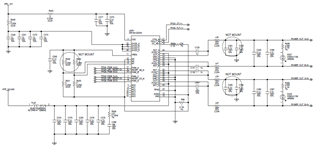
We are debugging DRV8412 board. But I found DRV8412 went to following damage status sometimes:

The first output channel (Pin5-7) is abnormal - No PWM output. But the second output channel (Pin15-17) is normal output with PWM we control. The FLT and OT are both in high level status.

So far we have found 3 pcs of DRV8412 with this same issue.

Could you help analyze which factor or operation trigger this issue? The solution will be very helpful and critical for our risk retirement. I attached circuit as below.

Thanks.

Xulong

  • Hello Xulong,

    Pin5, 7, 15 and 17 are input pins. Do you mean OUT_C and OUT_D don't follow Pin 5 and Pin 7 PWM input?

    I saw BST_x capacitor is 1uF. On the datasheet, the value is 100nF. Would you change four BST_x capacitors from 1uF to 100nF?

    Regards,

    Wang Li

  • Hi Wang Li,

    Thanks for your response. Yes, I mean OUT_C and OUT_D don't follow Pin 5 and Pin 7 PWM input and I suspect the DRV8412 was damaged. 

    As for the BST capacitor, we have to use 1uF because our control frequency is 1kHz and I check the datasheet which described 1uF should be ok for this application:

    For applications with lower than 10-kHz switching frequency and not to trigger BST_UVP protection, a larger
    bootstrap capacitor can be used (for example, 1-μF capacitor for 800-Hz operation).

    We use CBC mode.

    Thanks.

    Xulong

  • Xulong,

    A quick look at your schematic shows that you did NOT add the series 5 ohm resistors as recommended in the datasheet for larger Bootstrap capacitors.  The statement below is right after the statement you make above.

    When using a bootstrap cap larger than 220 nF, it is recommended to add 5-Ω resistors between 12-V GVDD power supply and GVDD_X pins to limit the inrush current on the internal bootstrap circuitry

    Without these capacitors, you risk damaging the internal bootstrap circuit.

    Regards,

    Ryan

  • Yes, I knew that and I tried adding 5-ohm resistors between 12V and GVDD. But it doesn't work. Meanwhile, when I remove C248/C386/C385/C387, the failure rate is very low, but I still found a pcs of DRV8412 is damaged after running 12 hours in our real application. So I don't think it's a great way to resolve this issue.

    By the way, I still have one more question: why are all damaged channel pin5/6/7 channel (OUT_C&OUT_D) in all damaged DRV8412? The pin15/16/17 channels of all damaged chips are still very good. Could you please help give me some internal circuit mechanism explaining?

  • Xulong,

    "I tried adding 5-ohm resistors between 12V and GVDD. But it doesn't work"

    Do you mean the damage still same? Or, do you mean DRV8412 doesn't work.

    "why are all damaged channel pin5/6/7 channel (OUT_C&OUT_D) in all damaged DRV8412?"

    Are the Pin5, 7 input signals same as Pin15, ,17?

    "when I remove C248/C386/C385/C387, the failure rate is very low,"

    What is the output current? Would you share the part number of L36, L39, L45 and L47?

    Regards,

    Wang